Template Revision 2.15
Template Change history: - 2.14 to 2.15
- add excerpt macro to key features
- 2.13 to 2.14
- add fix table of content
- add table size as macro
- 2.12 to 2.13
- Changed controller Signals section
- Module: TRM Name always "TE Series Name" +TRM
Example: "TE0728 TRM" - Carrier: TRM Name usually "TEB Series Name" +TRM
Example: "TEB0728 TRM"
|
----------------------------------------------------------------------- |
Note for Download Link of the Scroll ignore macro: |
Overview
The Trenz Electronic TE0835 is an extended-grade module based on Xilinx Zynq UltraScale+ RFSoC. The module is equipped with 4x 8Gb DDR4 SDRAM Memory, 2x 512Mb SPI Flash Memory, USB2.0, Ethernet Transceiver and 2x Samtec Razor Beam Borard to Board (B2B) Connectors. The system controller CPLD is provided by Lattice MachXO2.
The Zynq UltraScale+ RFSoC family integrates key subsystems for multiband, multi-mode cellular radios and cable infrastructure (DOCSIS) into an SoC platform that contains a feature-rich 64-bitquad-core Arm Cortex-A53 and dual-core Arm Cortex-R5 based processing system.
Refer to http://trenz.org/te0835-info for the current online version of this manual and other available documentation.
Key Features
Note:
'description: Important components and connector or other Features of the module
→ please sort and indicate assembly options Key Features' must be split into 6 main groups for modules and mainboards: - SoC/FPGA
- Package: SFVC784
- Device: ZU2...ZU5*
- Engine: CG, EG, EV*
- Speed: -1LI, -2LE,*, **
- Temperature: I, E,*, **
- RAM/Storage
- Low Power DDR4 on PS
- Data width: 32bit
- Size: def. 2GB*
- Speed:***
- eMMC
- Data width: 8Bit
- size: def. 8GB *
- QSPI boot Flash in dual parallel mode (size depends on assembly version)
- Data width: 8bit
- size: def. 128MB *
- HyperRAM/Flash (optional, default not assembled)
- MAC address serial EEPROM with EUI-48™ node identity (Microchip 24AA025E48)
- On Board
- Lattice LCMXO2
- PLL SI5338
- Gigabit Ethernet transceiver PHY (Marvell Alaska 88E1512)
- Hi-speed USB2 ULPI transceiver with full OTG support (Microchip USB3320C)
- Interface
- 132 x HP PL I/Os (3 banks)
- ETH
- USB
- 4 GTR (for USB3, Sata, PCIe, DP)
- MIO for UART
- MIO for SD
- MIO for PJTAG
- JTAG
- Ctrl
- Power
- 3.3V-5V Main Input
- 3.3V Controller Input
- Variable Bank IO Power Input
- Dimension
- Notes
- * depends on assembly version
- ** also non low power assembly options possible
- *** depends on used U+ Zynq and DDR4 combination
Key Features' must be split into 6 main groups for carrier: - Modules
- TE0808, TE807, TE0803,...
- RAM/Storage
- On Board
- Interface
- E.g. ETH, USB, B2B, Display port
- Power
- E.g. Input supply voltage
- Dimension
|
- SoC/FPGA
- Package: FFVE1156, FSVE1156
- Device: ZU25, ZU27, ZU28, ZU43, ZU47, ZU48*
- Engine: DR
- Speed: -1, -L1, -2, -L2
- Temperature: E, I*
- RAM/Storage
- 4x 8Gb DDR4
- 2x 512Mb SPI Flash
- 2k I2C EEPROM
- On Board
- Lattice MachXO2 CPLD
- Programmable Clock Generator
- USB2.0 Transceiver
- Gigabit Ethernet Transceiver
- 3x Oscillators
- 4x User LEDs
- Interface
- 2x Samtec Razor Beam ST5 (2x80 pol) Board to Board Connectors
- Power
- Dimension
- Note
- * Different packages, speed and temperature range are available on assembly options
|
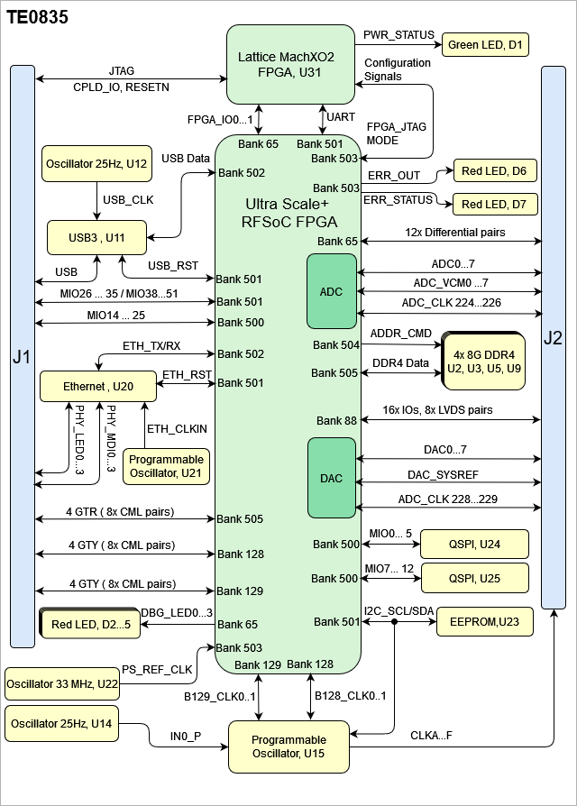
Block Diagram
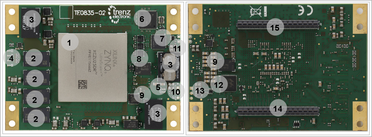
Main Components
Notes : - Picture of the PCB (top and bottom side) with labels of important components
- Add List below
|
- Xilinx UltraScale+ RFSoC, U1
- 8Gb DDR4 SDRAM, U2,U3,U5,U9
- Voltage Regulators, U4,U6,U7
- User Red LEDs, D2...5
- Error/Status Red LEDs, D6...7
- Programmable Glock Generator, U15
- Lattice MachXO2 CPLD, U31
- Dual SPI Flash, U24-U25
- USB2.0 Transceiver, U11
- Pin Header 3x1, J3 (not Soldered)
- Green LED, D1
- Gigabit Ethernet Transceiver, U20
- EEPROM, U23
- B2B Connectors, J1
- B2B Connectors, J2
Initial Delivery State
Notes : Only components like EEPROM, QSPI flash can be initialized by default at manufacture. If there is no components which might have initial data ( possible on carrier) you must keep the table empty |

Storage device name | Content | Notes |
|---|
2x SPI Flash | Not Programmed |
| | System Controller CPLD | Programmed |
| | EEPROM | Not Programmed |
| | 4x DDR4 SDRAM | Not Programmed |
| | Programmable Clock Generator | Not Programmed |
|
|
Configuration Signals
- Overview of Boot Mode, Reset, Enables.
|
Configuration must be set through CPLD,U31 by setting MODE0...3 signals.
MODE[3:0] | Boot Mode | Note |
|---|
0000 | PS_JTAG | Refer to CPLD Page | | 0001 | Quad SPI Flash | Refer to CPLD Page | | 0101 | SD Card | Refer to CPLD Page |
|
The reset pin is active low.
Signal | B2B | I/O | Note |
|---|
RESETN | J1-36 | Input | Pulled up to 3.3V_CPLD |
|
Signals, Interfaces and Pins
Notes : - For carrier or stand-alone boards use subsection for every connector type (add designator on description, not on the subsection title), for example:
- For modules which needs carrier use only classes and refer to B2B connector if more than one is used, for example
|
Board to Board (B2B) I/Os
FPGA bank number and number of I/O signals connected to the B2B connector:
| FPGA Bank | B2B Connector | Number of I/Os | Voltage Level | Notes |
|---|
| Bank 500 | J1 | 12x Single Ended | 1.8V | MIO14...25 | | Bank 501 | J1 | 20x Single Ended | 1.8V | MIO26...51 | | Bank 505 | J1 | 18x Single Ended, 9x Differential pairs | 0.85V | EXT_CLKIN_PSMGT, RX/TX0...3 | | Bank 128 | J1 | 2x Differnetial CLK Input, 8x Differential Transceiver | -- | B128_CLK, RX/TX0...3 | | Bank 129 | J1 | 2x Differnetial CLK Input 8x Differential Transceiver | -- | B129_CLK, RX/TX0...3 | | Bank 65 | J2 | 24x Single Ended, 12x Differential pairs | 1.8V | HP Bank | | Bank 88 | J2 | 16x Single Ended, 8x Differential pairs | 3.3V | HD Bank | | ADC | J2 | 16x Single Ended, 8x Differential pairs 4x Differential Clocks | Variable |
| | DAC | J2 | 16x Single Ended, 8x Differential pairs 3x Differential Clocks | Variable |
|
|
JTAG Interface
JTAG access to the Xilinx UltraScale+ MPSoC is through B2B connector JM1. JTAG signals routed directly through the CPLD to FPGA. Access between CPLD and FPGA can be multiplexed via JTAGEN (logical one for CPLD, logical zero for FPGA) on B2B. When the CPLD_JTAGEN is 0 or off, it provides FPGA access and when it is 1 or ON, it provides CPLD access.
JTAG Signal | B2B Connector |
|---|
| JTAG_TMS | J1-24 | | JTAG_TDI | J1-20 | | JTAG_TDO | J1-18 | | JTAG_TCK | J1-22 |
|
MIO Pins
you must fill the table below with group of MIOs which are connected to a specific components or peripherals, you do not have to specify pins in B2B, Just mention which B2B is connected to MIOs. The rest is clear in the Schematic. Example: | MIO Pin | Connected to | B2B | Notes |
|---|
| MIO12...14 | SPI_CS , SPI_DQ0... SPI_DQ3 SPI_SCK | J2 | QSPI |
|
| MIO Pin | Connected to | B2B | Notes |
|---|
| MIO0...12 | SPI FLash, U24-U25 | - | Dual SPI FLash | | MIO13 | LED Green, D1 | - | 3.3V_CPLD | | MIO14...25 | FPGA Bank 500,U1 | J1 | PSMIO | | MIO26...27 | FPGA Bank 501,U1 | J1 | PSMIO | | MIO28...29 | CPLD, U31 | - | UART_TX, UART_RX | | MIO30...31 | FPGA Bank 501, U1 | J1 | PSMIO | | MIO32...33 | EEPROM,U23 | - | I2C_SCL, I2C_SDA | | MIO34...35 | FPGA Bank 501,U1 | J1 | PSMIO | | MIO36 | Gigabit ETH, U20 | - | ETH_RST | | MIO37 | USB2.0, U11 | - | USB_RST | | MIO38...51 | FPGA Bank 501, U1 | J1 | PSMIO | | MIO52...62 | USB2.0, U11 | - | USB | | MIO63...77 | Gigabit ETH, U20 | - | ETH |
|
Test Points
you must fill the table below with group of Test Point which are indicated as TP in a schematic. If there is no Test Point remarked in the schematic, delet the Test Point section. Example: | Test Point | Signal | B2B | Notes |
|---|
| 10 | PWR_PL_OK | J2-120 |
|
|
| Test Point | Signal | Connected to | Notes |
|---|
| TP1 | CLKOUT | Voltage Regulator, U7 |
| | TP2 | PLL_RSTN | Programmable Clock Generator, U15 |
| | TP4 | CPLD_JTAGEN | B2B, J1 CPLD, U31 |
| | TP5 | JTAG_TDO | B2B, J1 CPLD, U31 |
| | TP6 | JTAG_TDI | B2B, J1 CPLD, U31 |
| | TP7 | JTAG_TCK | B2B, J1 CPLD, U31 |
| | TP8 | JTAG_TMS | B2B, J1 CPLD, U31 |
| | TP9 | GND | GND |
| | TP10...11 | IO_L1P_AD15P_88, O_L4N_AD12N_88 | FPGA Bank 88, U1 |
| | TP12 | VIN | B2B, J1 |
| | TP13...14 | GND | GND |
| | TP15...16 | MIO32-MIO33 | EEPROM,U23 FPGA Bank 501, U1 |
| | TP17 | GND | GND |
| | TP18 | ADC_AVCC | LDO Voltage Regulator, U8 |
| | TP19 | ADC_AVCCAUX | LDO Voltage Regulator, U10 |
| | TP20 | 3.3V_CPLD | CPLD, U31 B2B, J1 |
| | T21 | CPLD_JT AGEN | B2B, J1 CPLD, U31 |
|
|
On-board Peripherals
Notes : - add subsection for every component which is important for design, for example:
- Two 100 Mbit Ethernet Transciever PHY
- USB PHY
- Programmable Clock Generator
- Oscillators
- eMMCs
- RTC
- FTDI
- ...
- DIP-Switches
- Buttons
- LEDs
|
Notes : In the on-board peripheral table "chip/Interface" must be linked to the corresponding chapter or subsection |
Quad SPI Flash Memory
Notes : Minimum and Maximum density of quad SPI flash must be mentioned for other assembly options. |
The TE0835 is a Dual SPI Flash module equipped with two SPI Flash U24, U25 connecfted to PSMIO FPGA bank 500.
| MIO Pin | Schematic | U24 Pin | U25 Pin | Notes |
|---|
| MIO0 | MIO0_QSPI | CLK | - |
| | MIO1 | MIO1_QSPI | DO | - |
| | MIO2 | MIO2_QSPI | nWP | - |
| | MIO3 | MIO3_QSPI | nHOLD | - |
| | MIO4 | MIO4_QSPI | DI | - |
| | MIO5 | MIO5_QSPI | nCS | - |
| | MIO7 | MIO5_QSPI | - | nCS |
| | MIO8 | MIO5_QSPI | - | DI |
| | MIO9 | MIO5_QSPI | - | DO |
| | MIO10 | MIO5_QSPI | - | nWP |
| | MIO11 | MIO5_QSPI | - | nHOLD |
| | MIO12 | MIO5_QSPI | - | CLK |
|
|
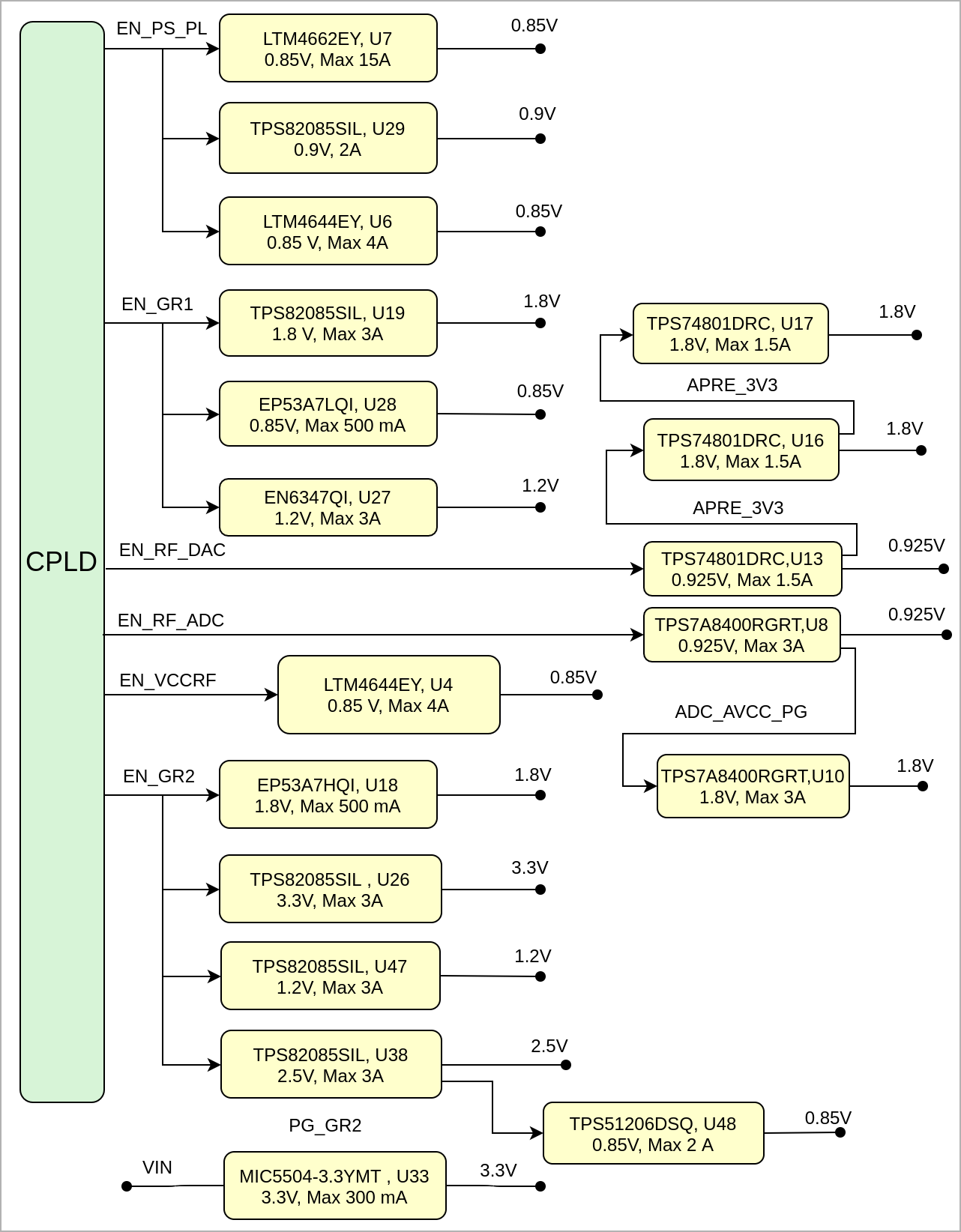
System Controller CPLD
The System Controller CPLD (U31) is provided by Lattice Semiconductor LCMXO2-460HC. The CPLD provides JTAG routing, boot mode, User IOs, LEDs, firmware and power management access. For more information please refer to the TE0835 CPLD page.
| Schematic/Pin | Connected to | Description | Note |
|---|
| MODE0...3 | FPGA Bank 503, U1 | Boot Mode |
| | POR_B | FPGA Bank 503, U1 | Programming Status | Pulled up | | PORG_B | FPGA Bank 503, U1 | Programming Status | Pulled up | | INIT_B | FPGA Bank 503, U1 | Configuration initialization | Pulled up | | DONE | FPGA Bank 503, U1 | Configuration Done Status | Pulled up | | F_TCK | FPGA Bank 503, U1 | FPGA JTAG |
| | F_TDI | FPGA Bank 503, U1 | FPGA JTAG |
| | F_TMS | FPGA Bank 503, U1 | FPGA JTAG |
| | F_TDO | FPGA Bank 503, U1 | FPGA JTAG |
| | JTAG_TDO | B2B, J1 | CPLD JTAG |
| | JTAG_TMS | B2B, J1 | CPLD JTAG |
| | JTAG_TDI | B2B, J1 | CPLD JTAG |
| | JTAG_TCK | B2B, J1 | CPLD JTAG |
| | CPLD_JTAGEN | B2B, J1 | CPLD JTAG Enable |
| | CPLDIO0...3 | B2B, J1 | CPLD IOs |
| | RESETN | B2B, J1 | Reset |
| | MIO13 | LED Green, D1 | 3.3V_CPLD |
| | MIO28 | FPGA Bank 501, U1 | UART_TX |
| | MIO29 | FPGA Bank 501, U1 | UART_RX |
| | FPGA_IO0...1 | FPGA Bank 65, U1 | IOs |
| | EN_PS_PL | Voltage Regulators, U6, U7, U29 | PS/PL Enable Signals | Pulled Down | | EN_GR1 | Voltage Regulators, U19, U27, U28 | MGTAVTT, PSLL | Pulled Down | | EN_GR2 | Voltage Regulators, U38, U18, U38 | PS_MGTRAVTT, 3.3, DDR2.5V | Pulled Down | | EN_RF_ADC | Voltage Regulators, U8 | Enable ADC | Pulled Down | | PG_RF_DAC | Voltage Regulators, U17 | ADC Power Good Status | Pulled Down | | PG_PS_PL | Voltage Regulators, U6, U7, U29 | PS/PL Power Good Status | Pulled Down | | EN_RF_DAC | Voltage Regulators, U13 | Enable DAC | Pulled Down | | PG_RF_DAC | Voltage Regulators, U10 | DAC Power Good Status | Pulled Down |
|
USB2.0
The TE0835 is equipped with a USB2.0, U11.
| U11 Pin | Schematic | Connected to | Notes |
|---|
| RESETB | USB0_RST | FPGA Bank 501, U1 |
| | VDDIO | 1.8V | 1.8V |
| | CPEN | USB0_CPE | B2B, J1 |
| | VBUS | USB0_VBUS | B2B, J1 |
| | ID | USB0_ID | B2B, J1 |
| | DP | USB0_D_P | B2B, J1 |
| | DM | USB0_D_N | B2B, J1 |
| | REFCLK | USB_CLK | Oschillator, U12 |
| | STP | USB0_STP | FPGA Bank 502, U1 |
| | NXT | USB0_NXT | FPGA Bank 502, U1 |
| | DIR | USB0_DIR | FPGA Bank 502, U1 |
| | CLKOUT | USB_CLK | Oschillator, U12 |
| | DATA0...7 | USB0_DATA0...8 | FPGA Bank 502, U1 |
|
|
Ethernet
The module TE0835 is equipped with a Gigabit Ethernet Transceiver, U20.
| U20 Pin | Signal Name | Connected to | Signal Description | Note |
|---|
| MDIO | ETH_MDIO | FPGA Bank 502, U1 | Data Management |
| | MDC | ETH_MDC | FPGA Bank 502, U1 | Data Management clock reference for the serial interface |
| | TX_CLK | ETH_TXCK | FPGA Bank 502, U1 | Transmit Clock |
| | TX_CTRL | ETH_TXCTL | FPGA Bank 502, U1 | Transmit Control |
| | TXD0...3 | ETH_TXD0...3 | FPGA Bank 502, U1 | Transmit Data |
| | RX_CLK | ETH_RXCK | FPGA Bank 502, U1 | Receive Clock |
| | RX_CTRL | ETH_RXCTL | FPGA Bank 502, U1 | Receive Control |
| | RXD0...3 | ETH_RXD0...3 | FPGA Bank 502, U1 | Receive Data |
| | RESETn | ETH_RST | FPGA Bank 501, U1 | Ethernet reset, Active low. |
| | XTAL_IN | ETH_XTAL_IN | Oscillator, U21 | Reference Clock |
| MDI0...3 | PHY_MDI0...3 | B2B, J1 | Media Dependent Interface 0...3 |
| | LED0...1 | PHY_LED0...1 | B2B, J1 | LED output |
| | LED/INT | PHY_LED2 | B2B, J1 | LED interrupt |
|
|
EEPROM
The module TE0835 has an EEPROM IC (U23) connected to PSMIO FPGA Bank 501.
| MIO Pin | Schematic | U23 Pin | Notes |
|---|
| MIO32 | MIO32_I2C1_SCL | SCL |
| | MIO33 | MIO33_I2C1_SDA | SDA |
|
|
| MIO Pin | I2C Address | Designator | Notes |
|---|
| MIO32...33 | 0xA1 | U23 |
|
|
LEDs
| Designator | Color | Connected to | Active Level | Note |
|---|
| D1 | Green | MIO13 | Active High | 3.3V CPLD | | D2...5 | Red | DBG_LED0...3 | Active Low | User LED | | D6 | Red | ERR_OUT | Active High |
| | D7 | Red | ERR_STATUS | Active High |
|
|
DDR4 SDRAM
Notes : Minimum and Maximum density of DDR3 SDRAM must be mentioned for other assembly options. (pay attention to supported address length for DDR3) |
The TE0835 SoM has 4x 1 Gigabyte volatile DDR4 SDRAM IC for storing user application code and data.
- Part number: K4A8G165WB
- Supply voltage: 1.2 V
Speed: 2400 Mbps
Temperature: -40 ~ 95 °C
Clock Sources
| Designator | Description | Frequency | Note |
|---|
| U14, U21 | MEMS Oscillator | 25MHz |
| | U22 | MEMS Oscillator | 33.33 MHz |
| | Y1 | Crystal Oscillator | 54 MHz |
| | U12 | MEMS Oscillator | 52MHz |
| | U15 | Programmable Clock Generator | Variable |
|
|
Programmable Clock Generator
There is a Silicon Labs I2C programmable clock generator on-board (U10) in order to generate reference clocks for the module. Programming can be done using I2C via PIN header J3. The I2C Address is 0x69.

U15 Pin
| Signal | Connected to | Direction | Note |
|---|
IN0 | IN0_P | Oscillator, U14 | Input |
| | IN1 | - | N.C | - |
| | IN2 | EXT_CLK_IN1 | B2B,J2 | Input |
| | IN3 | - | N.C |
|
| nRST | PLL_RSTN | FPGA Bank 65,U1 | Input |
| | SCL | MIO32_I2C1_SCL | Pin Header, J3 | Input | I2C | | SDA | MIO33_I2C1_SDA | Pin Header, J3 | Input | I2C | | OUT0 | CLKC | B2B,J2 | Output | Differential Clock | | OUT1 | CLKB | B2B,J2 | Output | Differential Clock | | OUT2 | CLKA | B2B,J2 | Output | Differential Clock | | OUT3 | CLKD | B2B,J2 | Output | Differential Clock | | OUT4 | CLKE | B2B,J2 | Output | Differential Clock | | OUT5 | CLKF | B2B,J2 | Output | Differential Clock | | OUT6 | B128_CLK0 | FPGA Bank 128,U1 | Output |
| | OUT7 | B129_CLK0 | FPGA Bank 129,U1 | Output |
| | OUT8 | CLK8 | FPGA Bank 65,U1 | Output |
| | OUT9 | PSMGT_100MHZ | FPGA Bank 505,U1 | Output |
| | OUT9A | CLK0A_100MHZ | B2B, J1 | Output |
|
|
Power and Power-On Sequence
In 'Power and Power-on Sequence' section there are three important digrams which must be drawn: - Power on-sequence
- Power distribution
- Voltage monitoring circuit
|
Power Supply
Power supply with minimum current capability of 2.5A for system startup is recommended.
Power Consumption
| Power Input Pin | Typical Current |
|---|
| VIN (5V) | TBD* |
|
* TBD - To Be Determined
Power Distribution Dependencies
Power-On Sequence
Power Rails
| Power Rail Name | B2B J1 Pin | B2B J2 Pin | Direction | Notes |
|---|
| VIN | 1,2,3,4,5,6,8 | - | Input |
| | PSBATT | 14 | - | Input |
| | 3.3V_CPLD | 16 | - | Output |
|
|
Bank Voltages
| Schematic Name | | Notes |
|---|
| Bank 65 HP | VCCO_65 | 1.8V |
| | Bank 503 PSCONFIG | VCCO_PSIO3_503 | 1.8V |
| | Bank 88 HD | VCCO_88 | 3.3V |
| | Bank 128 GTY | MGTAVCC | 0.9V |
| | Bank 129 GTY | MGTAVCC | 0.9V |
| | Bank 500 PSMIO | VCCO_PSIO0_500 | 1.8V |
| | Bank 501 PSMIO | VCCO_PSIO0_501 | 1.8V |
| | Bank 502 | VCCO_PSIO0_502 | 1.8V |
| | Bank 504 PSDDR | VCCO_PSDDR_504 | 1.2V |
| | Bank 505 PSGTR | PS_MGTRAVCC | 0.85V |
|
|
Board to Board Connectors
- This section is optional and only for modules.
use "include page" macro and link to the general B2B connector page of the module series, For example: 6 x 6 SoM LSHM B2B Connectors

|

Technical Specifications
Absolute Maximum Ratings
| Symbols | Description | Min | Max | Unit |
|---|
| VIN | Input Supply Voltage | 0 | 5 | V | | T_STG | Storage Temperature | -40 | 95 | °C |
|
Recommended Operating Conditions
Operating temperature range depends also on customer design and cooling solution. Please contact us for options.
| Parameter | Min | Max | Units | Reference Document |
|---|
| VIN | 4.5 | 5.5 | V | See Schematic | | T_OPR | -40 | 85 | °C | See USB2.0 Datasheet |
|
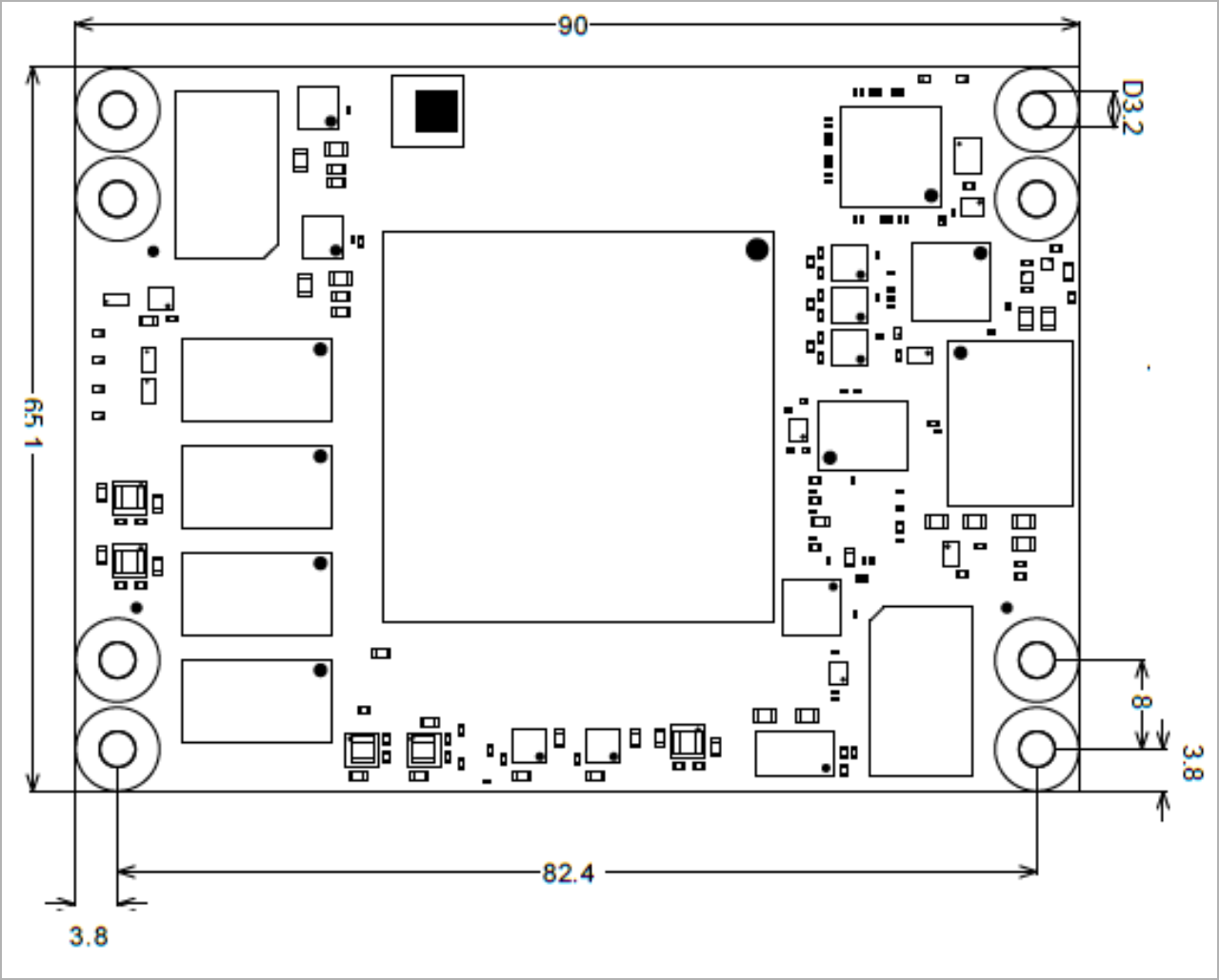
Physical Dimensions
PCB thickness: 1.65 mm.
Currently Offered Variants
Revision History
Hardware Revision History
| Date | Revision | Changes | Documentation Link |
|---|
| 2019-11-05 | REV01 | Initial Release | REV01 | | 2020-06-17 | REV02 | 1. Added a VRP resistor on bank 65; 2. LDO U33 is changed on ADP7102ACPZ; 3. Signal FPGA IO0 is connected on AE18 pin of FPGA; 4. Signal DBG_LED3 is connected on AD18 pin of FPGA; 5. Signal MIO13_25 connected to J1 pin 33 instead MIO25. 6. Resistor R84 is removed; 7. LED D1 moved on edge of PCB; 8. Added THT testpoints J4 on CPLD_JTAGEN, R76 was removed; 9. Signals B49_XX_X are renamed in B88_XX_X; 10. C241 is changed on 1nF; 11. Length of CLK signals on RFADC and RFDAC are adjusted; 12. Wrong connection on U8 is fixed (PCB); 13. Wrong connection PGOOD1 pin of U7 is fixed; 14. R17 is changed from 35,5K to 33K for VCC_PL_PS correction. | REV02 |
|
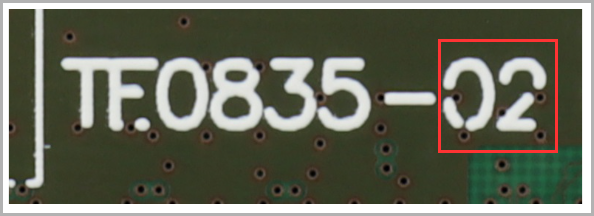
Hardware revision number can be found on the PCB board together with the module model number separated by the dash.
| |
|
Document Change History
- Note this list must be only updated, if the document is online on public doc!
- It's semi automatically, so do following
Add new row below first Copy "Page Information Macro(date)" Macro-Preview, Metadata Version number, Author Name and description to the empty row. Important Revision number must be the same as the Wiki document revision number Update Metadata = "Page Information Macro (current-version)" Preview+1 and add Author and change description. --> this point is will be deleted on newer pdf export template - Metadata is only used of compatibility of older exports
|
| Date | Revision | Contributor | Description |
|---|
| | 
| | | 2021-12-21 | v.58 | John Hartfiel | - Bugfix B2B section
- Replace GTH with GTY
| | 2021-05-28 | v.55 | John Hartfiel | Style update - Bugfix PDF Link
- Key features update
| | 2020-11-23 | v.51 | Pedram Babakhani | | -- | all | 
| |
|
Disclaimer