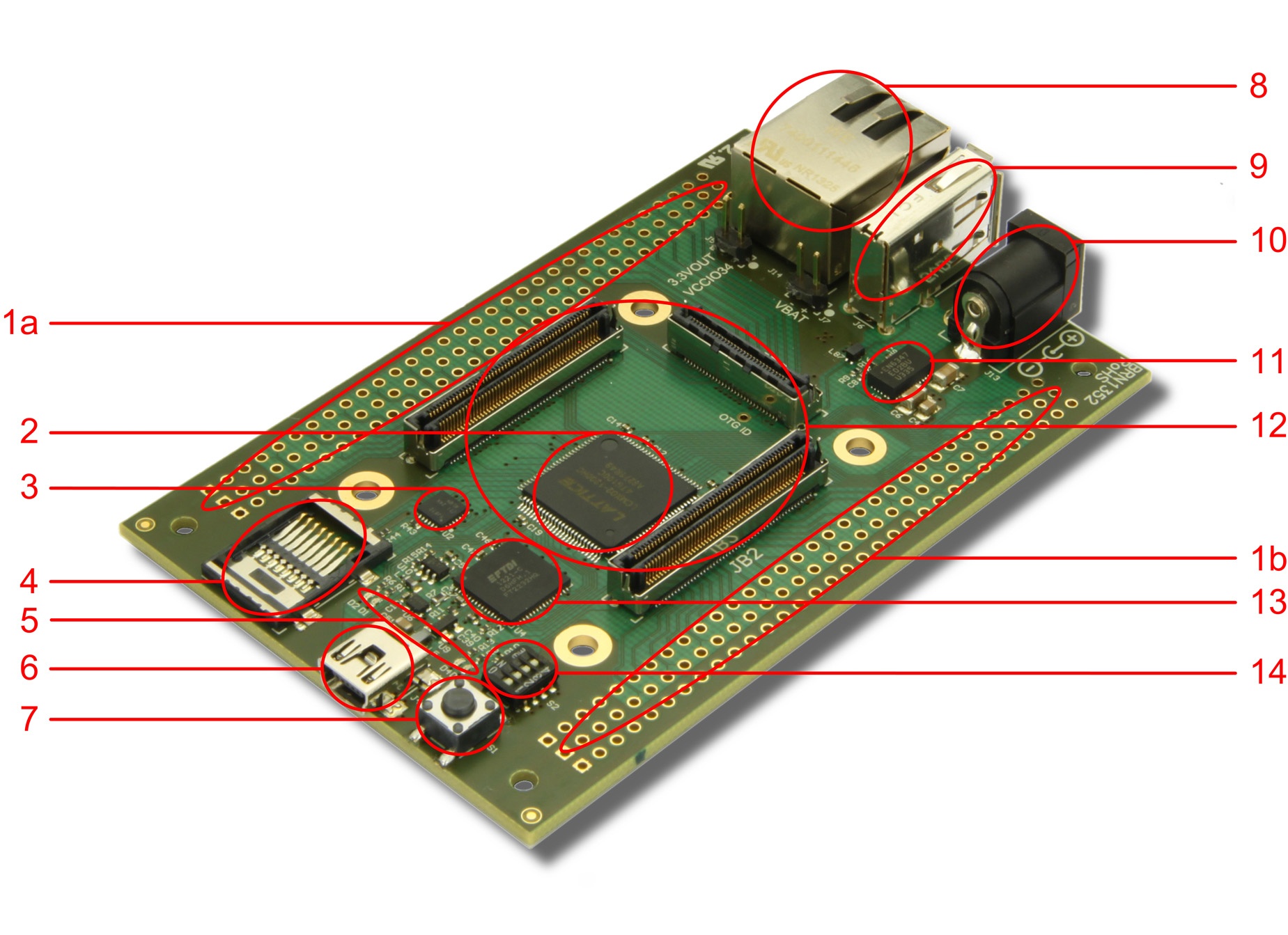
Figure 1: TE0703 (REV 01).
Overview
Features
- VG96 Connectors (Mounting Holes and Solder Pads)
- Carrier Controller CPLD (Lattice LCMXO2-1200HC)
SD Card level-shifter
- Micro SD Card Connector
- LEDs
- Mini USB Connector FT2232H
- User Push Button
- RJ45 GbE Connector
- USB Host Connector
- Barrel jack for 5V Power Supply
- 4A High-Efficiency DC-DC Step-Down Converter for 3.3V Power Supply
- Trenz 4x5 Module Socket (3x Samtec LSHM Series Connectors)
- USB JTAG and UART Interface (FTDI FT2232H), compatible with Xilinx Tools
- DIP Switch
Note: TE0703 must be powered by a 5V power supply!
User I/O Connectors
Note: VCCIO for FPGA banks is has no default fixed connection to power supply. Those the bank VCCIO must be supplied to externally, or optionally 0 ohm resistors can be soldered onto TE0703 to set fixed 3.3V voltages.
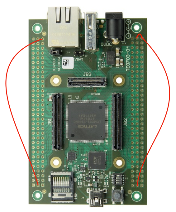
Example wiring that powers ALL banks with 3.3V - those connections should be present on the base board, in this drawing 3 banks are have VCCIO supplied over connector and 4th bank is connected to 3.3V with jumper J5.
TE0715-30 modification
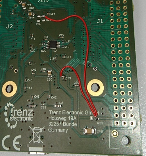
REMOVE jumper J5, add wires as on picture for VCCIO=1.8V for all banks.
UART
FT2232H USB interface Channel B is normally used as UART, in default CPLD configuration UART pins are routed to Module connector to location of default UART pins.
| FT2232H Channel B | B2B | TE0715 | TE0720 | TE0710 | TE0711 | TE0712 | TE0713 | TE0741 | Notes |
|---|---|---|---|---|---|---|---|---|---|
| TXD | JM1.92 | MIO14 | MIO14 | A8 | N17 | P16 | A10 | J21 | Module input |
| RXD | JM1.85 | MIO15 | MIO15 | B8 | R10 | U18 | C11 | G24 | Module output |
LEDS
Two LED's (those closer to mini-USB Connector) are connected to the 4x5 B2B Connector pins. Those LEDs can be controlled by FPGA Module.
| LED | Net Name | Color | B2B/Module | TE0710 | TE0711 | TE0712 | TE0713 | TE0715 | TE0720 | TE0741 |
|---|---|---|---|---|---|---|---|---|---|---|
| D3 | FLED1 | Red | JM2.100 | U8 | F5 | J16 | U8 | H6 | U7 | U21 |
| D4 | FLED2 | Green | JM2.89 | K6 | J5 | M17 | K6 | H5 | R7 | Y20 |
The bank where LED's are is not powered when TE0703 is used in standalone mode. VCCIO for this bank must be supplied back to the TE0703 connectors. TE0703 header Pin J2.B1 must have some valid I/O voltage or the LED's will not be lit. To connect 3.3V to this bank install 0R or solder bridge to empty place of R26 on the bottom of the PCB.
If the Bank where LED's are has VCCIO 1.8V then the LED's will lit with very low intensity.
Two LED's closer to the micro SD Card are connected to CPLD and not Module Connectors, their function depends on the CPLD Version.
| Notes | |||
|---|---|---|---|
| D1 | ULED1 | Red | FTDI UART Receive activity |
| D2 | ULED2 | Green | FTDI UART Transmit activity |
Default function of the User LED's. Note the function of this LEDs is controlled by the CPLD and can be changed.
I2C Level Shifter
TE0703 has a I2C level shifter IC on-board, there are however no I2C devices on TE0703. Those pins that go through level shifter can be used I2C bus, or as GPIO.
| Net | B2B/Module | TE0715 | TE0720 | TE0710 | TE0711 | TE0712 | TE0713 | TE0741 | |
|---|---|---|---|---|---|---|---|---|---|
| SCL | JM1.95 | MIO10 | MIO10 | R10 | M13 | T21 | B9 | L22 | |
| SDA | JM1.93 | MIO11 | MIO11 | L18 | L18 | Y22 | A9 | K21 |
Micro SD Card Socket
The Micro SD Card Socket do not include a Card detect signal and Write Protect signal. It is not directly connected to the 4x5 B2B Connector pins, but through a SDIO port expander, TI TXS02612. This device is used for voltage translation, due to the different voltage levels between Micro SD Card and MIO Bank 501 on the Zynq 7000 . (The Micro SD Card is 3.3V, but the MIO Bank 501 is set to 1.8V.)
| Signal Name | Description | Net Name | B2B/Module | TE0715 | TE0720 |
|---|---|---|---|---|---|
| DATA[3] | Data | DAT3 | JM1.17 | MIO45 | MIO45 |
| DATA[2] | Data | DAT2 | JM1.19 | MIO44 | MIO44 |
| DATA[1] | Data | DAT1 | JM1.21 | MIO43 | MIO43 |
| DATA[0] | Data | DAT0 | JM1.23 | MIO42 | MIO42 |
| CMD | Command | CMD | JM1.25 | MIO41 | MIO41 |
| CLK | Clock | S_CLK | JM1.27 | MIO40 | MIO40 |
DIP Switch settings
| 4 | MODE = LOW | MODE = HIGH | Module "MODE" Pin level, select between boot-modes (SPI <> SD for Zynq modules) |
| 3 | Normal mode | CC Update mode | JTAG Select: fixed function can not be changed |
| 2 | |||
| 1 |
Function of MODE pin is module dependent!
Carrier Controller Update Mode
Carrier Controller JTAG port is enabled by setting switch 3 on DIP switch S2 on TE0703 to "OFF" position. This setting is only useful when updating Carrier Controller firmware! In this mode Module JTAG is not accessible.
Switch 3 on DIP switch S2 must be moved to "ON" position for normal operation! Otherwise the JTAG on the module would not be accessible at all.
Configuring B34 Bank Supply for TE0720 Zynq SoC Module
J5 Jumper can be used to power TE0720 bank 34 from TE0720 3.3V output rail. If J5 is installed TE0720 will boot also in the case bank 34 supply is not delivered from the VG96 /Pin headers. If TE0720 bank supply of 3.3V is required it is recommended to insert the jumper. Optionally, 3.3V or any other valid IO voltage can be supplied from the TE0703 pins.
Use with TE0715
Care should be taken with TE0715-30, all I/O should be set to 1.8V
Backup Battery Supply (VBAT connector)
J7 provides two pins (+/-) to supply battery backup voltage to TE0720. If not required leave open.
Ensure to connect the supply battery to jumper J7 with correct polarity!
Revision History
REV 04
- corrected Pull up on U10
- PCB cosmetic changes
Document Change History
| date | revision | authors | description |
|---|---|---|---|
| 2014-02-12 | Work in progress | ||
All |
Data Privacy
Please also note our data protection declaration at https://www.trenz-electronic.de/en/Data-protection-Privacy
Document Warranty
The material contained in this document is provided “as is” and is subject to being changed at any time without notice. Trenz Electronic does not warrant the accuracy and completeness of the materials in this document. Further, to the maximum extent permitted by applicable law, Trenz Electronic disclaims all warranties, either express or implied, with regard to this document and any information contained herein, including but not limited to the implied warranties of merchantability, fitness for a particular purpose or non infringement of intellectual property. Trenz Electronic shall not be liable for errors or for incidental or consequential damages in connection with the furnishing, use, or performance of this document or of any information contained herein.
Limitation of Liability
In no event will Trenz Electronic, its suppliers, or other third parties mentioned in this document be liable for any damages whatsoever (including, without limitation, those resulting from lost profits, lost data or business interruption) arising out of the use, inability to use, or the results of use of this document, any documents linked to this document, or the materials or information contained at any or all such documents. If your use of the materials or information from this document results in the need for servicing, repair or correction of equipment or data, you assume all costs thereof.
Copyright Notice
No part of this manual may be reproduced in any form or by any means (including electronic storage and retrieval or translation into a foreign language) without prior agreement and written consent from Trenz Electronic.
Technology Licenses
The hardware / firmware / software described in this document are furnished under a license and may be used /modified / copied only in accordance with the terms of such license.
Environmental Protection
To confront directly with the responsibility toward the environment, the global community and eventually also oneself. Such a resolution should be integral part not only of everybody's life. Also enterprises shall be conscious of their social responsibility and contribute to the preservation of our common living space. That is why Trenz Electronic invests in the protection of our Environment.
REACH, RoHS and WEEE
REACH
Trenz Electronic is a manufacturer and a distributor of electronic products. It is therefore a so called downstream user in the sense of REACH. The products we supply to you are solely non-chemical products (goods). Moreover and under normal and reasonably foreseeable circumstances of application, the goods supplied to you shall not release any substance. For that, Trenz Electronic is obliged to neither register nor to provide safety data sheet. According to present knowledge and to best of our knowledge, no SVHC (Substances of Very High Concern) on the Candidate List are contained in our products. Furthermore, we will immediately and unsolicited inform our customers in compliance with REACH - Article 33 if any substance present in our goods (above a concentration of 0,1 % weight by weight) will be classified as SVHC by the European Chemicals Agency (ECHA).
RoHS
Trenz Electronic GmbH herewith declares that all its products are developed, manufactured and distributed RoHS compliant.
WEEE
Information for users within the European Union in accordance with Directive 2002/96/EC of the European Parliament and of the Council of 27 January 2003 on waste electrical and electronic equipment (WEEE).
Users of electrical and electronic equipment in private households are required not to dispose of waste electrical and electronic equipment as unsorted municipal waste and to collect such waste electrical and electronic equipment separately. By the 13 August 2005, Member States shall have ensured that systems are set up allowing final holders and distributors to return waste electrical and electronic equipment at least free of charge. Member States shall ensure the availability and accessibility of the necessary collection facilities. Separate collection is the precondition to ensure specific treatment and recycling of waste electrical and electronic equipment and is necessary to achieve the chosen level of protection of human health and the environment in the European Union. Consumers have to actively contribute to the success of such collection and the return of waste electrical and electronic equipment. Presence of hazardous substances in electrical and electronic equipment results in potential effects on the environment and human health. The symbol consisting of the crossed-out wheeled bin indicates separate collection for waste electrical and electronic equipment.
Trenz Electronic is registered under WEEE-Reg.-Nr. DE97922676.
Overview
Content Tools