| Company | Trenz Electronic GmbH |
|---|---|
| PCN Number | PCN-20260219 |
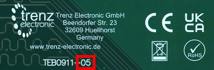
| Title | TEB0911-04 to TEB0911-05 Hardware Revision Change |
| Subject | Hardware Revision Change |
| Issue Date | 2026-02-20 |
Products Affected
This change affects all Trenz Electronic TEB0911 boards: TEB0911-04*.
Affected Product | Replacement |
|---|---|
| TEB0911-04-9BEX1MA | TEB0911-05-9BEX1MA |
| TEB0911-04-BBEX1MA | TEB0911-05-BBEX1MA |
Changes
#1 Changed DCDC EN5311QI (U50, U84, U72, U80) to MPM3834CGPA-Z and adapted power circuit.
Type: Schematic Change
Reason: EOL of Component.
Impact: None. Increased output current capability. Minor changes in electrical characteristics.
#2 Changed DCDC EN6347QI (U52, U55, U58, U62, U64, U66, U70, U74, U79) to MPM3860GQW-Z and adapted power circuit.
Type: Schematic Change
Reason: EOL of Component.
Impact: None. Increased output current capability. Minor changes in electrical characteristics.
#3 Increased voltage of five rails.
- Changed voltage from 1.05 V to 1.14 V and adapted power net name accordingly from PL_GT_1V05 to PL_GT_1V14.
- Changed voltage from 1.05 V to 1.14 V and adapted power net name accordingly from PL_GT2_1V05 to PL_GT2_1V14.
- Changed voltage from 1.05 V to 1.14 V and adapted power net name accordingly from PS_GT_1V05 to PS_GT_1V14.
- Changed voltage from 1.35 V to 1.4 V and adapted power net name accordingly from PL_GT_1V35 to PL_GT_1V4.
- Changed voltage from 1.35 V to 1.4 V and adapted power net name accordingly from PL_GT2_1V35 to PL_GT2_1V4.
Type: Schematic Change
Reason: Increase drop out voltage margin.
Impact: None.
#4 Changed ethernet connection.
- Removed ethernet PHY signals (PHY_LED0, PHY_LED1, PHY_LED2, LED_1A, LED_2A, LED_2B) from system controller.
- Renamed ethernet PHY signals (PHY_LED0 → ETH0_LINK_ACTn, PHY_LED1 → ETH0_LINK_MIDn, PHY_LED2 → ETH0_LINK_MAXn).
- Added schmitt trigger (U103 ... U105) between ethernet PHY (U20) and RJ45 (J13) LEDs to show signals ETH0_LINK_ACTn, ETH0_LINK_MIDn and ETH0_LINK_MAXn.
- Changed RJ45 and USB connector (J13) from 7497110616 to 2250576-1 and adapted corresponding circuit accordingly.
- Changed status LED colours:
- J13D: Yellow → Green
- J13E: Orange → Yellow
Type: Schematic Change
Reason: Improve and harmonize ethernet circuit behaviour.
Impact: Function for LED signals changed. System controller firmware changed.
#5 Changed fan architecture.
- Added fan connector (J14, J37 ... J41).
- Added MOSFET (T1 ... T6).
- Connected fan speed control signal (FMCA_PWM, FMCB_PWM, FMCC_PWM, FMCD_PWM, FMCE_PWM, FMCF_PWM) between MOSFETs (T1 ... T6) for fan connectors (J14, J37 ... J41) and system controller.
- Connected fan sensor signal (FMCA_SENSE, FMCB_SENSE, FMCC_SENSE, FMCD_SENSE, FMCE_SENSE, FMCF_SENSE) between MOSFETs (T1 ... T6) for fan connectors (J14, J37 ... J41) and system controller.
- Changed fan (M1 ... M6) from AFB04512MA to CFM-5010-13-22.
- Added mechanical connector (JX1 ... JX6).
- Added mechanical contacts (CONT1 ... CONT24).
Type: Schematic Change
Reason: Improve cooling solution.
Impact: None. Improved cooling possibilities.
#6 Modified FMC power good handling.
- Added supervisor (U110 ... U115) for FMC power supplies.
- Disconnected signals (FMCA_PG_C2M, FMCB_PG_C2M, FMCC_PG_C2M, FMCD_PG_C2M, FMCE_PG_C2M, FMCF_PG_C2M) from system controller and connected them to supervisors (U110 ... U115).
- Connected signals (SC_A_PG_C2M, SC_B_PG_C2M, SC_C_PG_C2M, SC_D_PG_C2M, SC_E_PG_C2M, SC_F_PG_C2M) from system controller to supervisors (U110 ... U115).
- Added input protection diodes (D21 ... D26) for supervisors (U110 ... U115).
Type: Schematic Change
Reason: Follow FMC specification.
Impact: None. Control power good behaviour dependent on power rails.
#7 Changed crystal (Y4) SC12S-12.5PF20PPM to crystal (Y2) LFXTAL050789REEL and modified crystal circuit accordingly.
Type: Schematic Change
Reason: Improve manufacturing process.
Impact: None.
#8 Added pull-up resistor (R377 ... R380) for signal (MIO3 [HOLD#], MIO2 [WP#], MIO11 [HOLD#], MIO10 [WP#]) for flash (U24, U25).
Type: Schematic Change
Reason: Implement proper initial conditions regardless on the state of FPGA and used flash.
Impact: None. Minor changes in electrical characteristics.
#9 Added protection diode (D20).
Type: Schematic Change
Reason: Improve input protection.
Impact: Improved input protection.
#10 Changed diode AOZ8808DI-03 (U28, U68, U88) to AOZ8S311UD4-03.
Type: Schematic Change
Reason: Part is NRND.
Impact: None. Minor changes in electrical characteristics.
#11 Changed crystal (Y3) from CX3225SB26000D0FFFCC to FL2600176.
Type: BOM Change
Reason: Improve temperature range.
Impact: Increased operating temperature range from -20 °C - 70 °C to -40 °C - 85 °C. Minor changes in electrical characteristics.
#12 Changed resistor (R92) from 33 Ohm to 220 Ohm.
Type: BOM Change
Reason: Improve SDIO interface behaviour.
Impact: None.
#13 Changed resistor (R17) from 1 kOhm to 2.2 kOhm.
Type: Schematic Change
Reason: Follow recommendation of manufacturer.
Impact: None. Minor changes in electrical characteristics.
#14 Changed resistor (R49, R283, R328) from 4.99 kOhm to 100 Ohm.
Type: BOM Change
Reason: Improve signal quality.
Impact: Improved signal quality.
#15 Added decoupling capacitor (C699 ... C705).
Type: Schematic Change
Reason: Improve 3.3V_SD power rail stability.
Impact: None. Minor changes in electrical characteristics.
#16 Changed 470 nF capacitor (C612, C613) from 0402 to 0201.
Type: Schematic Change
Reason: BOM Optimization.
Impact: None. Minor changes in electrical characteristics.
#17 Changed power net name from DDR_PG to PG_DDR_1V2.
Type: Schematic Change
Reason: Improve net name description.
Impact: None.
#18 Removed track-it traceability pad (S/N) from PCB.
Type: Schematic Change
Reason: EOL of Component.
Impact: None.
#19 Added UKCA- and RoHS-logo.
Type: PCB Change
Reason: Improve product classification identification.
Impact: None.
#20 Added test point (TP41, TP42, TP47, TP48).
Type: Schematic Change
Reason: Voltage and system monitoring improvement.
Impact: None.
Method of Identification
The revision number is shown on the top side of the PCB.
Production Shipment Schedule
This change takes place with immediate effect. If the new revision is not suitable for your application and still the former revision of the board is needed, please contact us.
Contact Information
If you have any questions related to this PCN, please contact Trenz Electronics Technical Support at
- forum.trenz-electronic.de
- wiki.trenz-electronic.de
- support%trenz-electronic.de (subject = PCN-20260219)
phone
national calls: 05741 3200-0
international calls: 0049 5741 3200-0
Disclaimer
Any projected dates in this PCN are based on the most current product information at the time this PCN is being issued, but they may change due to unforeseen circumstances. For the latest schedule and any other information, please contact your local Trenz Electronic sales office, technical support or local distributor.
This PCN follows JEDEC Standard J-STD-046.
Overview
Content Tools