| Company | Trenz Electronic GmbH |
|---|---|
| PCN Number | PCN-20261019 |
| Title | TEI0005-02 to TEI0005-03 Hardware Revision Change |
| Subject | Hardware Revision Change |
| Issue Date | 2026-10-20 |
Products Affected
This change affects all Trenz Electronic TEI0005 SoMs: TEI0005-02*.
Affected Product | Replacement |
|---|---|
| TEI0005-02 | TEI0005-03 |
Changes
#1 Changed red LED (D1) to RGB LED and adapted surrounding circuit accordingly.
- Changed LED (D1) from LTST-C191KRKT to 150044M155260.
- Connected red LED to FT2232H (U3) signal ADBUS7 (pin 20) and ACBUS5 (pin 27) and SMD pad 12.
- Connected green LED to FT2232H (U3) signal ACBUS6 (pin 28) and SMD pad 11.
- Connected blue LED to FT2232H (U3) signal ACBUS7 (pin 29) and SMD pad 10.
Type: Schematic Change
Reason: Visual feedback for power and JTAG activity (according to Altera USB Blaster III FPGA Development Cable User Guide).
Impact: Check whether new mechanical position fits your requirements. Minor changes in electrical characteristics.
#2 Changed green LED (D2) from LTST-C191KGKT to SML-P11MTT86R.
Type: Schematic Change
Reason: BOM Optimization.
Impact: Check whether new mechanical position fits your requirements. Minor changes in electrical characteristics.
#3 Connected UART activity LED (D2) signal "UART_ACT" to SMD pad 9.
Type: Schematic Change
Reason: Improve status indication for new carrier card designs.
Impact: None.
#4 Changed SMD pad 1 connection from ADBUS4 to ADBUS6 and adapted surrounding circuits accordingly.
- Pulled-up ADBUS4 signal to 3.3V via resistor R13.
- Pulled-up ADBUS6 signal to 3.3V via resistor R7 [REV03] and connected it to SMD pad 1 via buffer U2.
Type: Schematic Change
Reason: Improve device handling.
Impact: SMD pad 1 functionality changed to use processor reset instead of test reset (according to Altera USB Blaster III FPGA Development Cable User Guide).
#5 Added ENABLE connection from SMD pad 3 to ACBUS4 via voltage level translation (T1, R14, R16) and pulled it down via resistor (R15).
Type: Schematic Change
Reason: Improve functionality.
Impact: Improved functionality.
#6 Changed transceiver (U2, U4) connection and adapted surrounding circuits accordingly.
- Changed VCCA from 3.3V to VREF.
- Changed VCCB from VREF to 3.3V.
- Changed signals accordingly.
- Changed reference voltage for signal OEN from 3.3V to VREF.
- Reordered IO signals.
- Pulled-down TCK_C signal via resistor R17.
- Changed resistor R6 from 10 kOhm to 100 kOhm.
Type: Schematic Change
Reason: Improve power rail handling.
Impact: Improved power rail handling.
#7 Removed signal BCBUS0 from transceiver U4 completely.
Type: Schematic Change
Reason: Remove not needed signal from pinout.
Impact: Removed auto-transmit enable control for RS485 serial applications using TXDEN (BDBUS0).
#8 Added decoupling capacitor C9 for 3.3V power rail.
Type: Schematic Change
Reason: Improve power rail integrity.
Impact: None. Minor changes in electrical characteristics.
#9 Changed 1 µF capacitor from X5R to X7R.
Type: Schematic Change
Reason: Improve temperature behaviour.
Impact: None. Minor changes in electrical characteristics.
#10 Removed chamfer on PCB edge and added orientation mark.
Type: PCB Change
Reason: Improve manufacturing process.
Impact: None.
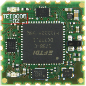
Method of Identification
The revision number is printed on the top side of the PCB.
Production Shipment Schedule
From May 2027, after old stock is gone. If the new revision is not suitable for your application and still the former revision of the board is needed, please contact us.
Contact Information
If you have any questions related to this PCN, please contact Trenz Electronics Technical Support at
- forum.trenz-electronic.de
- wiki.trenz-electronic.de
- support%trenz-electronic.de (subject = PCN-20261019)
phone
national calls: 05741 3200-0
international calls: 0049 5741 3200-0
Disclaimer
Any projected dates in this PCN are based on the most current product information at the time this PCN is being issued, but they may change due to unforeseen circumstances. For the latest schedule and any other information, please contact your local Trenz Electronic sales office, technical support or local distributor.
This PCN follows JEDEC Standard J-STD-046.
Overview
Content Tools