| Company | Trenz Electronic GmbH |
|---|---|
| PCN Number | PCN-20230621 |
| Title | TEF0007-02A to TEF0007-03 Hardware Revision Change |
| Subject | Hardware Revision Change |
| Issue Date | 2023-06-27 |
Products Affected
This change affects all Trenz Electronic TEF0007 SoMs: TEF0007-02A*.
Affected Product | Replacement |
|---|---|
| TEF0007-02A | TEF0007-03-B2C-1-A |
Changes
#1 Changed DCDC EN6347QI (U16) to MPM3840GQV-Z and adapted power circuit.
Type: Schematic Change
Reason: EOL of Component.
Impact: None. Minor changes in electrical characteristics.
#2 Changed DCDC EP5357HUI (U19) to LDO MIC5504-2.5YM5.
Type: Schematic Change
Reason: EOL of Component.
Impact: None. Decreased current output capability. Minor changes in electrical characteristics.
#3 Changed DCDCs TPS82085SIL (U7, U20, U25) to MPM3834CGPA-Z and adapted power circuit.
Type: Schematic Change
Reason: BOM Optimization.
Impact: None. Minor changes in electrical characteristics.
#4 Changed load switch from TPS27082LDDCR (Q1) to MP5077GG-Z and adapted circuit.
Type: Schematic Change
Reason: BOM Optimization.
Impact: None. Increased current output capability. Minor changes in electrical characteristics.
#5 Changed high side switch (U6, U21) TPS2051BDGN to MIC2544-1YMM.
Type: Schematic Change
Reason: BOM Optimization.
Impact: None. Increased current output capability. Minor changes in electrical characteristics.
#6 Changed configuration flash (U2) S25FL256SAGBHI20 to MT25QL256ABA8E12-1SIT.
Type: Schematic Change
Reason: BOM Optimization
Impact: Design have to be updated accordingly.
#7 Changed clock (U26) from SiT8008AI-73-XXS-50.000000E to SiT8008BI-73-XXS-50.000000E.
Type: Schematic Change
Reason: Use new clock revision.
Impact: None.
#8 Removed clock generator Si5345A-B-GM (U10), clock oscillator SiT8008BI-73-18S-25.000000E (U11), crystal CX3225SB54000 (Y2) and replaced five clock signals by clock oscillators (Y1, Y2, Y3, Y4, Y5). Adapted clock oscillator circuits. Removed I2C interface at FPGA (U1) bank 34 pin U2 and pin U1 and adapted circuit.
Type: Schematic Change
Reason: EOL of Component.
Impact: Clock signals CLK0_P/N, CLK1_P/N, CLK2_P/N, CLK3_P/N, GTCLK1_P/N are completely removed. Differential clock signal CLK6_P/N changed to 25 MHz single ended (CLK6_P) clock oscillator (Y4). Clock signal GTCLK0_P/N changed to 125 MHz clock oscillator (Y5). Clock signal GT_CLK2_P/N changed to 135 MHz clock oscillator (Y1). Clock signal CLK4_P/N changed to 135 MHz clock oscillator (Y2). Clock signal CLK5_P/N changed to 125 MHz clock oscillator (Y3).
#9 Changed ferrid bead BKP0603HS121-T (L3, L5, L7, L9, L10, L11, L13, L14) to MPZ0603S121HT000.
Type: Schematic Change
Reason: EOL of Component.
Impact: None.
#10 Added 100 Ohm termination resistor (R91) assembly option for clock signals GT_HP_CK_P/N.
Type: Schematic Change
Reason: Add option for external termination resistor usage.
Impact: None.
#11 Changed connection for resistors R4 and R5 from power net to GND net and changed standard assembly status to fitted.
Type: Schematic Change
Reason: Follow Display Port Standard.
Impact: None.
#12 Changed net name SOURCEDP_PWRCON to SOURCEDP_CONFIG2 and added assembly option to connect Config2 source side to GND (R72).
Type: Schematic Change
Reason: Follow Display Port Standard.
Impact: None.
#13 Renamed net "PG_0V85" to net "PG_1V0".
Type: Schematic Change
Reason: Correct voltage level in name according to voltage rail level.
Impact: None.
#14 Changed resistors R31 and R41 to 330 Ohm.
Type: BOM Change
Reason: Decrease LED brightness.
Impact: None.
#15 Changed voltage rating from 16 V to 100 V and size from 0402 to 1206 for capacitor (C14, C48).
Type: Schematic Change
Reason: Improve capacitors characteristics for capacitor functionality.
Impact: None. Improved characteristics.
#16 Added testpoints TP5...TP14 and TP16...TP20.
Type: Schematic Change
Reason: Improve testability.
Impact: None.
#17 Length matched all differential signals smaller than 0.1 mm.
Type: PCB Change
Reason: Improve signal integrity.
Impact: None. Minor trace length change. The trace length for new revision will be available in TEF0007 series pinout generator. Please check if change in trace length still matches your requirements. Adaption of carrier may be necessary.
#18 Added UKCA logo.
Type: PCB Change
Reason: Required for export to UK.
Impact: None.
#19 Updated components from library.
Type: Schematic Change
Reason: Use latest component data.
Impact: None.
#20 Added legal notices, revision history, system and power overview. Removed clock overview. Updated page count and order.
Type: Documentation Update
Reason: Documentation improvement.
Impact: None.
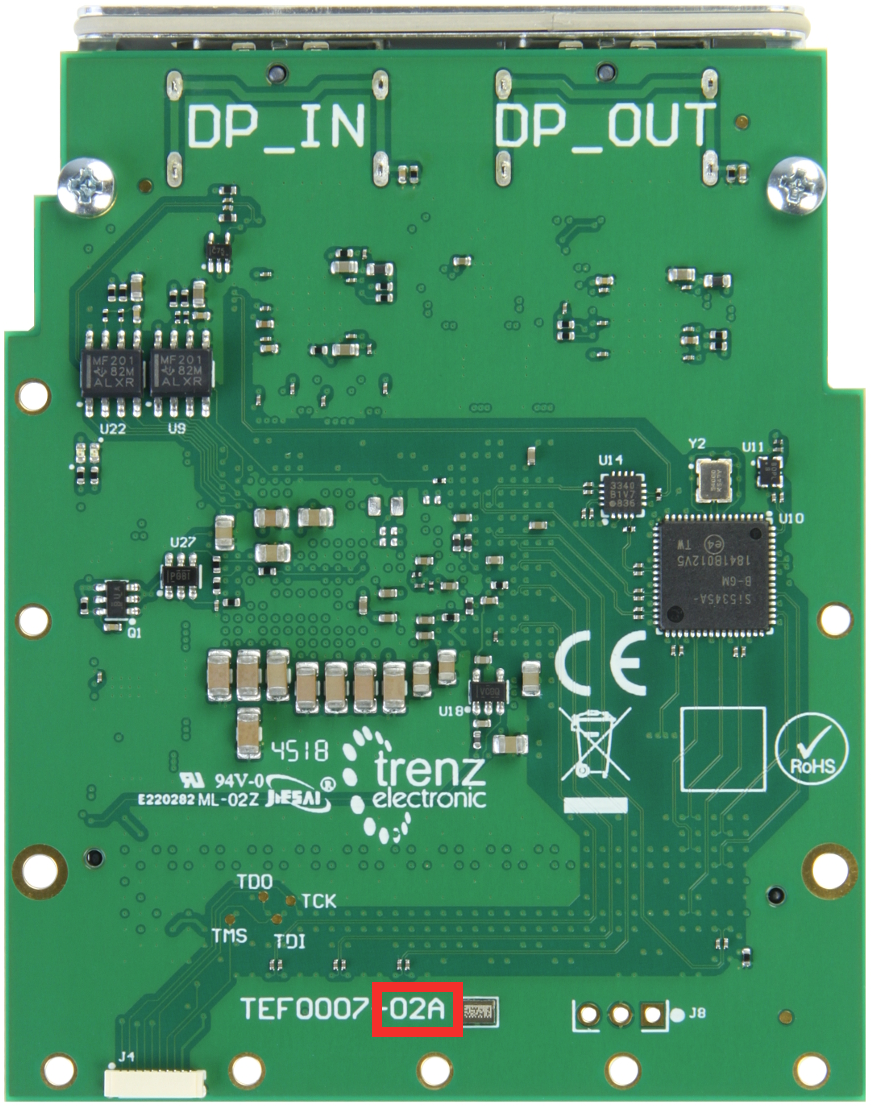
Method of Identification
The revision number is shown on the bottom side of the PCB.
Production Shipment Schedule
This change takes place with immediate effect. If the new revision is not suitable for your application and still the former revision of the board is needed, please contact us.
Contact Information
If you have any questions related to this PCN, please contact Trenz Electronics Technical Support at
- forum.trenz-electronic.de
- wiki.trenz-electronic.de
- support%trenz-electronic.de (subject = PCN-20230621)
phone
national calls: 05741 3200-0
international calls: 0049 5741 3200-0
Disclaimer
Any projected dates in this PCN are based on the most current product information at the time this PCN is being issued, but they may change due to unforeseen circumstances. For the latest schedule and any other information, please contact your local Trenz Electronic sales office, technical support or local distributor.
This PCN follows JEDEC Standard J-STD-046.
Overview
Content Tools