| Company | Trenz Electronic GmbH |
|---|---|
| PCN Number | PCN-20220725 |
| Title | TE0820-04 to TE0820-05 Hardware Revision Change |
| Subject | Hardware Revision Change |
| Issue Date | 2022-08-04 |
Products Affected
This change affects all Trenz Electronic TE0820 SoMs of Revision 04: TE0820-04*.
Affected Product | Replacement |
|---|---|
| TE0820-04-2AE21MA | TE0820-05-2AE21MA |
| TE0820-04-2AE21MAZ | TE0820-05-2AE21MAZ |
| TE0820-04-2AI21MA | TE0820-05-2AI21MA |
| TE0820-04-2AI21MAZ | TE0820-05-2AI21MAZ |
| TE0820-04-2AI21MC | TE0820-05-2AI21MC |
| TE0820-04-2AI21MCZ | TE0820-05-2AI21MCZ |
| TE0820-04-2BE21MA | TE0820-05-2BE21MA |
| TE0820-04-2BE21MAJ | TE0820-05-2BE21MAJ |
| TE0820-04-2BE21MAZ | TE0820-05-2BE21MAZ |
| TE0820-04-2BE21ML | TE0820-05-2BE21ML |
| TE0820-04-2BE21MLZ | TE0820-05-2BE21MLZ |
| TE0820-04-2BI21MA | TE0820-05-2BI21MA |
| TE0820-04-2BI21MAZ | TE0820-05-2BI21MAZ |
| TE0820-04-2BI21ML | TE0820-05-2BI21ML |
| TE0820-04-2BI21MLZ | TE0820-05-2BI21MLZ |
| TE0820-04-3AE21MA | TE0820-05-3AE21MA |
| TE0820-04-3AE21MAZ | TE0820-05-3AE21MAZ |
| TE0820-04-3BE21MA | TE0820-05-3BE21MA |
| TE0820-04-3BE21MAZ | TE0820-05-3BE21MAZ |
| TE0820-04-3BE21ML | TE0820-05-3BE21ML |
| TE0820-04-3BE21MLZ | TE0820-05-3BE21MLZ |
| TE0820-04-3BI21ML | TE0820-05-3BI21ML |
| TE0820-04-3BI21MLZ | TE0820-05-3BI21MLZ |
| TE0820-04-4AE21MA | TE0820-05-4AE21MA |
| TE0820-04-4AE21MAZ | TE0820-05-4AE21MAZ |
| TE0820-04-4AI21MC | TE0820-05-4AI21MC |
| TE0820-04-4AI21MCZ | TE0820-05-4AI21MCZ |
| TE0820-04-4AI21MI | TE0820-05-4AI21MI |
| TE0820-04-4BI21PL | TE0820-05-4BI21PL |
| TE0820-04-4BI21PLZ | TE0820-05-4BI21PLZ |
| TE0820-04-4DE21MA | TE0820-05-4DE21MA |
| TE0820-04-4DE21MAZ | TE0820-05-4DE21MAZ |
| TE0820-04-4DI21MA | TE0820-05-4DI21MA |
| TE0820-04-4DI21MAZ | TE0820-05-4DI21MAZ |
| TE0820-04-5DI21MA | TE0820-05-5DI21MA |
| TE0820-04-5DI21MAZ | TE0820-05-5DI21MAZ |
| TE0820-04-5DR21MA | TE0820-05-5DR21MA |
| TE0820-04-5DR21MAZ | TE0820-05-5DR21MAZ |
| TE0820-04-S002C1 | TE0820-05-S002C1 |
Changes
#1 Changed EN6363QI to MPM3860GQW-Z for U5.
Type: Schematic Change
Reason: EOL of Component
Impact: None. Minor changes in electrical characteristics.
#2 Changed TPS27082LDDCR to MP5077GG-Z for U28.
Type: Schematic Change
Reason: BOM Optimization
Impact: None. Minor changes in electrical characteristics.
#3 Changed BKP0603HS121-T to MPZ0603S121HT000 for L1, ... L5, L7, L9, ... L12.
Type: Schematic Change
Reason: EOL of Component
Impact: None. Minor changes in electrical characteristics.
#4 Improved decoupling capacitor structure.
Type: Schematic Change
Reason: Updated decoupling capacitor structure according to Xilinx recommendations.
Impact: None.
#5 Insert DDR4 testing option (R116, TP9).
Type: Schematic Change
Reason: Allow extended automatic DDR4 testing.
Impact: None.
#6 Changed AO7800 to BSD840NH6327XTSA1 for T1.
Type: Schematic Change
Reason: BOM Optimization
Impact: None. Minor changes in electrical characteristics.
#7 Added voltage detector BD39040MUF-CE2 (U30) and connected signal "PG_ALL" to CPLD (U21.5) and to testpoint TP12.
Type: Schematic Change
Reason: Power management improvement.
Impact: None. All power supplies are monitored.
#8 Changed SiT8008AI-73-XXS-52.000000E to SiT8008BI-73-XXS-52.000000E for U14.
Type: Schematic Change
Reason: Improve power management.
Impact: None.
#9 Changed reset, enable and power-up structure with resistor R95, added transistor T2, and added resistor R128.
Type: Schematic Change
Reason: Improve module reset, enable, and power-up.
Impact: Module reset, enable, and power-up handling is modified. That means that "EN1" signal from B2B connector enables DCDC U5 and can be monitored by CPLD U21 pin 27 (assembly option) (backward compatible mode with assembled resistor R95 and signal "EN1" as enable input), or that signal "EN1" only enables DCDC U5 and CPLD U21 pin 27 is connected to signal "POR_B" via voltage translator T2 (normal mode). Normal mode is standard. Therefore, please, verify that the module meets your requierements.
#10 Added voltage level translator U29 and resistor R129 as assembly option to connect signal "PHY_LED1" to SoC.
Type: Schematic Change
Reason: Connect both PHY signals to SoC.
Impact: None. Signal optional available at SoC (assembly option).
#11 Added resistors R130 and R131 to add pull-up/-down option for SoC "POR_OVERRIDE" signal.
Type: Schematic Change
Reason: Improvement to allow "POR_OVERRIDE" state change.
Impact: None. Assembly option with power override possible.
#12 Added diode D5 to protect manual reset input signal.
Type: Schematic Change
Reason: Improvement to protect reset input signal.
Impact: None.
#13 Updated components from library.
Type: Schematic Change
Reason: Use latest component data.
Impact: None.
#14 Change voltage divider R64 and R58.
Type: Schematic Change
Reason: Change reset voltage threshold from 0.74 V to 0.775 V.
Impact: None. Improve brown-out detection.
#15 Added resistor R132 as assembly option.
Type: Schematic Change
Reason: Added assembly option for DCI.
Impact: None.
#16 Change R92 to not assembled.
Type: BOM Change
Reason: R92 is not needed.
Impact: None. Not needed for x16 DDR4.
#17 Added power diagram page.
Type: Documentation Update
Reason: Power documentation improvement.
Impact: None.
Method of Identification
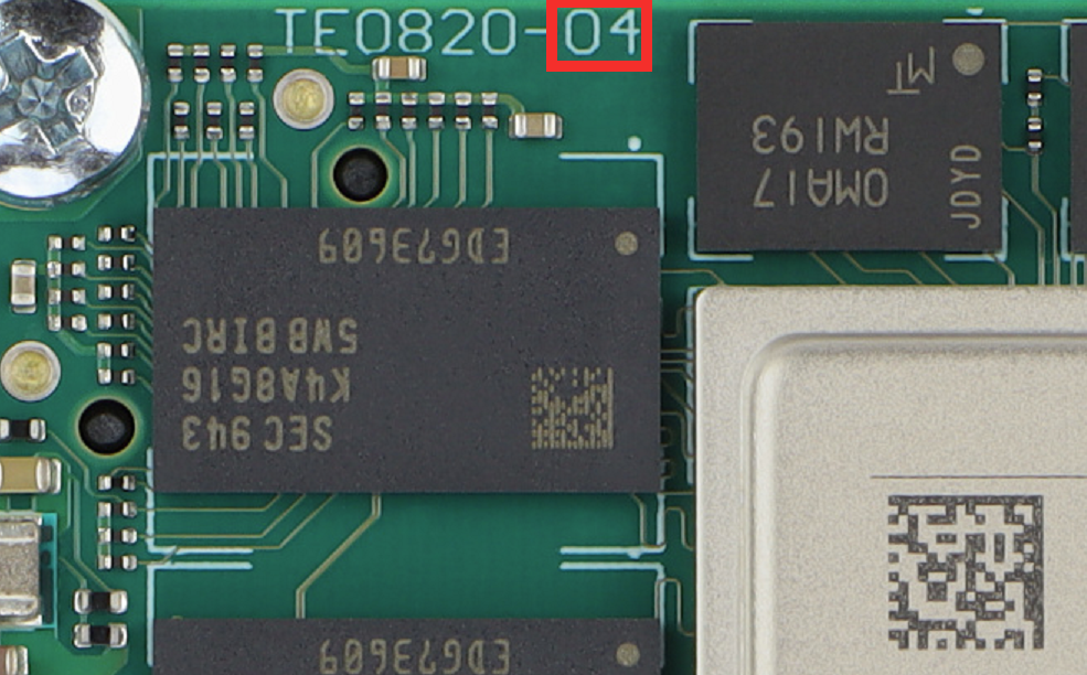
The revision number is printed on the top side of the PCB.
Production Shipment Schedule
This change takes place with immediate effect. If the new revision is not suitable for your application and still the former revision of the board is needed, please contact us.
Contact Information
If you have any questions related to this PCN, please contact Trenz Electronics Technical Support at
- forum.trenz-electronic.de
- wiki.trenz-electronic.de
- support%trenz-electronic.de (subject = PCN-20220725)
phone
national calls: 05741 3200-0
international calls: 0049 5741 3200-0
Disclaimer
Any projected dates in this PCN are based on the most current product information at the time this PCN is being issued, but they may change due to unforeseen circumstances. For the latest schedule and any other information, please contact your local Trenz Electronic sales office, technical support or local distributor.
This PCN follows JEDEC Standard J-STD-046.
