| Company | Trenz Electronic GmbH |
|---|---|
| PCN Number | PCN-20230327 |
| Title | TE0745-02 to TE0745-03 Hardware Revision Change |
| Subject | Hardware Revision Change |
| Issue Date | 2023-06-27 |
Products Affected
This change affects all Trenz Electronic TE0745 SoMs: TE0745-02*.
Affected Product | Changes | Replacement |
|---|---|---|
| TE0745-02-71I31-A | #2...#32 | TE0745-03-71I31-A |
| TE0745-02-72I31-A | #2...#32 | TE0745-03-72I31-A |
| TE0745-02-81C31-A | #2...#32 | TE0745-03-81C31-A |
| TE0745-02-91C31-A | #2...#32 | TE0745-03-91C31-A |
| TE0745-02-92I31-A | #2...#32 | TE0745-03-92I31-A |
| TE0745-02-93E31-A | #2...#32 | TE0745-03-93E31-A |
| TE0745-02-93E31-AK | #2...#32 | TE0745-03-93E31-AK |
| TE0745-02-71I31-AK | #2...#32 | TE0745-03-71I31-AK |
| TE0745-02-73E31-A | #2...#32 | TE0745-03-73E31-A |
| TE0745-02-81C31-AK | #2...#32 | TE0745-03-81C31-AK |
| TE0745-02-92I31-AK | #2...#32 | TE0745-03-92I31-AK |
| TE0745-02-82I31-A | #2...#32 | TE0745-03-82I31-A |
| TE0745-02-71I31-AZ | #1...#32 | TE0745-03-71I31-A |
| TE0745-02-72I31-AZ | #1...#32 | TE0745-03-72I31-A |
| TE0745-02-81C31-AZ | #1...#32 | TE0745-03-81C31-A |
| TE0745-02-91C31-AZ | #1...#32 | TE0745-03-91C31-A |
| TE0745-02-92I31-AZ | #1...#32 | TE0745-03-92I31-A |
| TE0745-02-93E31-AZ | #1...#32 | TE0745-03-93E31-A |
| TE0745-02-92I31-B | #2...#33 | TE0745-03-92I31-A |
Changes
#1 Changed DCDC MUN3CAD03-SE (U10, U13, U15, U19, U30, U31) to TPS82085SIL and adapted voltage divider resistors.
Type: BOM Change
Reason: TPS82085SIL availability.
Impact: Minor changes in electrical characteristics.
#2 Remove serial number S/N. Connected CPLD (U2) pin 20 to net "BOOTMODE".
Type: Schematic Change
Reason: EOL of Component.
Impact: None. Custom system controller firmware needs to be adapted if system controller (U2) pin 20 is used inside the firmware because pin functionality changes.
#3 Changed DCDC EN63A0QI (U4) to MP8869SGL-Z and adapted power circuit.
Type: Schematic Change
Reason: EOL of Component.
Impact: None. Minor changes in electrical characteristics.
#4 Added assembly option (Default: not fitted) to connect DCDC (U4) to I2C bus via resistors (R91 and R101) with I2C address 0x61.
Type: Schematic change
Reason: Optional MP8869SGL-Z I2C monitoring.
Impact: None. Consider possibly I2C address conflicts before connecting DCDC (U4) to I2C bus.
#5 Increased voltage rating from 6.3 V to 25 V for capacitors C108, C142, C147, C148, and C149.
Type: BOM change
Reason: Functionality change for capacitor C108 and BOM optimization.
Impact: None.
#6 Added diode D3 between signal "RST_IN_N" and "PS_1.8V" to protect manual reset input signal.
Type: Schematic Change
Reason: Protect manual reset pin.
Impact: None.
#7 Added series resistor R106 between CPLD (U2) pin 25 and signal "RST_IN_N".
Type: Schematic Change
Reason: Current limitation between different voltage regions.
Impact: None.
#8 Added option for diode D4 population between signal "INIT" and "PROG_B".
Type: Schematic Change
Reason: Keep FPGA in reset while signal "PROG_B" is low during initial power-up if necessary.
Impact: None.
#9 Changed clock (U33) from SiT8008AI-73-XXS-52.000000E to SiT8008BI-73-XXS-52.000000E.
Type: Schematic Change
Reason: Use new clock revision.
Impact: None.
#10 Added testpoints (TP1...TP43).
Type: Schematic Change
Reason: Voltage supervision improvement.
Impact: None.
#11 Added voltage detector BD39040MUF-CE2 (U22) and connected output to signal "PWR_PL_OK".
Type: Schematic Change
Reason: Power management improvement.
Impact: None.
#12 Added voltage detector BD39040MUF-CE2 (U20) and connected output to signal "PWR_PS_OK".
Type: Schematic Change
Reason: Power management improvement.
Impact: None. Refer to change #13.
#13 Added resistor R103 to optionally connect DCDC (U31) PG to handle signal "PWR_PS_OK" or use the voltage monitor U20 to handle signal "PWR_PS_OK".
Type: Schematic Change
Reason: Power management improvement.
Impact: None. Refer to change #12.
#14 Added pull-up resistor R73 for net "PWR_PL_OK".
Type: Schematic Change
Reason: Use pull-up resistor on SoM.
Impact: None.
#15 Changed supply voltage for VCCPLL from PL_1.8V to PS_1.8V.
Type: Schematic Change
Reason: Use AMD recommended power supply.
Impact: None.
#16 Tied DXP/DXN (U1 pins R14 and R13) directly to GND.
Type: Schematic Change
Reason: Use AMD recommendation for not used DXP/DXN pins.
Impact: None.
#17 Added soft start capacitor C62 option for TPS74401RGW (U8).
Type: Schematic Change
Reason: Added larger startup time option for DCDC U8.
Impact: None. For assembled capacitor larger startup times are possible.
#18 Added soft start capacitor C78 option for TPS74401RGW (U11).
Type: Schematic Change
Reason: Added larger startup time option for DCDC U11.
Impact: None. For assembled capacitor larger startup times are possible.
#19 Added decoupling capacitors C126...C131, C144, C150...C157.
Type: Schematic Change
Reason: Improve decoupling.
Impact: None.
#20 Changed voltage rating from 6.3 V to 10 V for 100 uF capacitors.
Type: BOM Change
Reason: BOM Optimization.
Impact: None.
#21 Changed voltage rating from 6.3 V to 16 V for 10 uF capacitors.
Type: BOM Change
Reason: BOM Optimization.
Impact: None.
#22 Changed voltage rating from 6.3 V to 10 V and size from 0402 to 0603 for capacitors C21 and C29.
Type: Schematic Change
Reason: Adapted capacitor voltage rating to possibly used voltage.
Impact: None.
#23 Changed size from 0201 to 0402 for 1 kOhm resistors R104 and R105.
Type: Schematic Change
Reason: BOM Optimization.
Impact: None.
#24 Added 100 Ohm termination resistor assemble option for MGT_REF_CLKs (R109 and R110).
Type: Schematic Change
Reason: Improvement.
Impact: None.
#25 Changed VCCADC_0 supply from VCCIO_0 to PL_1.8V.
Type: Schematic Change
Reason: Follow AMD recommendation for VCCADC_0 power supply.
Impact: None.
#26 Added UKCA logo.
Type: PCB Change
Reason: Requiered for export to UK.
Impact: None.
#27 Changed voltage divider R21 and R22 to set voltage threshold to 0.936 V for voltage monitor (U41).
Type: Schematic Change
Reason: Improve voltage monitoring.
Impact: None.
#28 Changed DDR clock termination resistor R9 placement position.
Type: PCB Change
Reason: Improve DDR clock termination.
Impact: None.
#29 Changed fiducials to standard fiducial type.
Type: Schematic Change
Reason: Use standard fiducials.
Impact: None.
#30 Signal trace lengths changed
Type: PCB change
Reason: Result of changes above.
Impact: Changed trace length have to be taken into account in existing designs. The trace length for new revision will be available in TE0745 series pinout generator. Please check if change in trace length still matches your requirements. Adaption of carrier may be necessary.
#31 Updated power overview.
Type: Documentation Update
Reason: Documentation improvement.
Impact: None.
#32 Removed page "ZYNQ.SchDoc" and added pages Legal Notices and System Overview.
Type: Documentation Update
Reason: Documentation improvement.
Impact: None.
#33 Change PCB color from black to standard green.
Type: PCB Update
Reason: Standardization.
Impact: None.
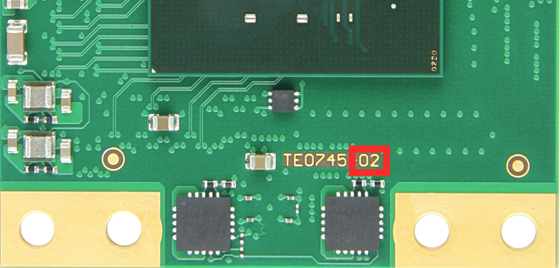
Method of Identification
The revision number is shown on the top side of the PCB.
Production Shipment Schedule
This change takes place with immediate effect. If the new revision is not suitable for your application and still the former revision of the board is needed, please contact us.
Contact Information
If you have any questions related to this PCN, please contact Trenz Electronics Technical Support at
- forum.trenz-electronic.de
- wiki.trenz-electronic.de
- support%trenz-electronic.de (subject = PCN-20230327)
phone
national calls: 05741 3200-0
international calls: 0049 5741 3200-0
Disclaimer
Any projected dates in this PCN are based on the most current product information at the time this PCN is being issued, but they may change due to unforeseen circumstances. For the latest schedule and any other information, please contact your local Trenz Electronic sales office, technical support or local distributor.
This PCN follows JEDEC Standard J-STD-046.
Overview
Content Tools