| Company | Trenz Electronic GmbH |
|---|---|
| PCN Number | PCN-20230619 |
| Title | TE0726-03 to TE0726-04 Hardware Revision Change |
| Subject | Hardware Revision Change |
| Issue Date | 2023-10-04 |
Products Affected
This change affects all Trenz Electronic TE0726 SoMs: TE0726-03*.
Affected Product | Replacement |
|---|---|
| TE0726-03-41I64-A | TE0726-04-41I94-A |
| TE0726-03-41C64-A | TE0726-04-41C94-A |
| TE0726-03-11C64-A | - |
| TE0726-03-41C74-Q | - |
| TE0726-03-41C74-R | - |
Changes
#1 Changed DCDC (U16, U17, U19, U20) from EN5311QI to MPM3834CGPA and adapted power circuit.
Type: Schematic Change
Reason: EOL of Component.
Impact: None. Increased current output capability. Minor changes in electrical characteristics.
#2 Changed DDR3 SDRAM (U8) from IS43TR16256BL-125KBLI to IS43TR16256ECL-125LB2LI.
Type: Schematic Change
Reason: Enable DDR3L ECC functionality.
Impact: Enable DDR3L ECC functionality. Firmware reflects it but custom firmware needs to be updated by customer.
#3 Added option to place pull-up (R157) or pull-down (R158) resistor for DDR3 pin M7.
Type: Schematic Change
Reason: Avoid floating signal situations for memory devices with M7 signal.
Impact: None.
#4 Connected DDR3 ECC I2C interface to I2C bus (Camera I2C or Header I2C) via I2C level shifter (U12) and adapted corresponding circuits (C120, C122, R153, R154, R156, and R159).
Type: Schematic Change
Reason: Enable DDR3L ECC functionality.
Impact: None. Minor changes in electrical characteristics.
#5 Added buffers (U24, U25) for voltage level translation for signal "DDR3-ERR_LV".
Type: Schematic Change
Reason: Enable DDR3L ECC functionality.
Impact: Enable DDR3L ECC functionality. Firmware reflects it but custom firmware needs to be updated by customer.
#6 Changed power-up sequencing.
Type: Schematic Change
Reason: Improved power-on sequence.
Impact: None. Updated power sequence.
#7 Added DIP switch (S1) and resistor (R152) to enable JTAG only boot mode.
Type: Schematic Change
Reason: QSPI programming problems with newer Vivado versions.
Impact: None. JTAG boot mode directly accessible. Fix QSPI programming problems with newer Vivado versions according to AR#00002 - QSPI Programming issues.
#8 Added 499 Ohm resistor (R162) and changed value for resistor (R141) from 2.61 kOhm to 499 Ohm to use signal "PUDC" as dual-purpose signal.
Type: Schematic Change
Reason: Enable dual-use option for signal "PUDC".
Impact: None. Firmware reflects it but custom firmware needs to be updated by customer.
#9 Changed HDMI CEC circuit (R140, D5) and removed HDMI CEC functionality via not assembled resistors (R140, R42), capacitor (C127) and diode (D5) and completely removed ferrid bead (L11).
Type: Schematic Change
Reason: Improve HDMI functionality.
Impact: If HDMI CEC is used in customer firmware, firmware needs to be modified or components needs to be assembled.
#10 Added diode (D7) and resistors (R155, R160) for voltage level translation for signal "DONE_LV" at CPLD (U11) to signal "DONE" at FPGA (U1).
Type: Schematic Change
Reason: Improve signal voltage level.
Impact: None.
#11 Added MIC bias power circuit (L12, C114, R151).
Type: Schematic Change
Reason: Alternative microphones usable.
Impact: None. Alternative microphones usable. Minor changes in electrical characteristics.
#12 Changed common mode filter SP5001-04TTG (D8, D9) to EMI8042MUTAG.
Type: Schematic Change
Reason: EOL of Component.
Impact: None. Minor changes in electrical characteristics.
#13 Changed ferrid bead (L1...L4, L6, L7, L9, L10) from BKP0603HS121-T to MPZ0603S121HT000.
Type: Schematic Change
Reason: EOL of Component.
Impact: None.
#14 Changed capacitors (C29, C32, C32) from 100 nF, 25 V, 0402 to 470 nF, 6.3 V, 0201.
Type: Schematic Change
Reason: BOM Optimization.
Impact: None.
#15 Changed resistors (R80, R81, R82) from 1.43 kOhm to 10 kOhm.
Type: Schematic Change
Reason: BOM Optimization.
Impact: None.
#16 Changed testpoint size from 0.8 mm to 1 mm diameter for testpoints (TP2, TP4, TP6, TP8...TP14).
Type: PCB Change
Reason: Use similar testpoints size for all testpoints.
Impact: None.
#17 Added testpoints TP15...TP20.
Type: PCB Change
Reason: Improve signal monitoring.
Impact: None.
#18 Changed fiducials to standard fiducial type.
Type: Schematic Change
Reason: Use standard fiducials.
Impact: None.
#19 Renamed signal name from "SPI-DQ0/M0" to "SPI-DQ0/M3".
Type: Schematic Change
Reason: Use AMD boot mode name convention.
Impact: None.
#20 Renamed signal name from "SPI-DQ3/M3" to "SPI-DQ3/M0".
Type: Schematic Change
Reason: Use AMD boot mode name convention.
Impact: None.
#21 Added legal notices, revision history, block and power diagram. Updated page count and order.
Type: Documentation Update
Reason: Documentation improvement.
Impact: None.
Method of Identification
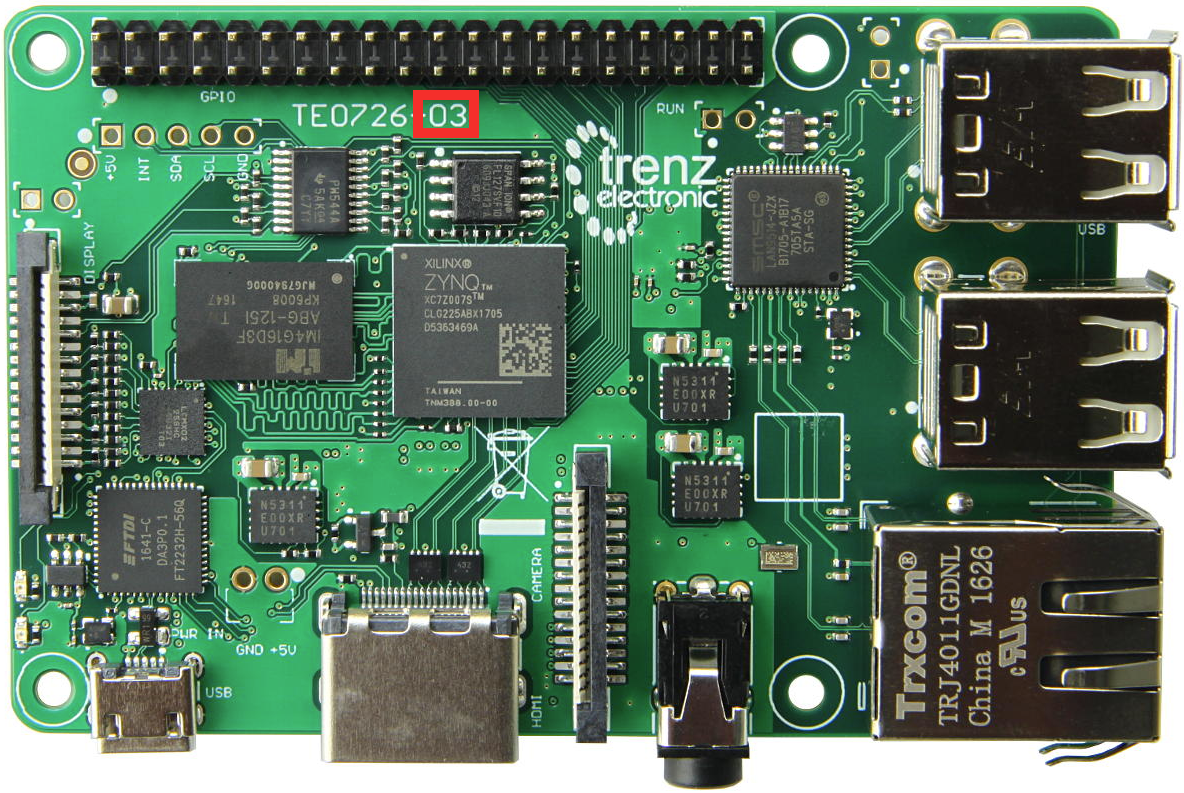
The revision number is shown on the top side of the PCB.
Production Shipment Schedule
From april 2024, after old stock is gone. If the new revision is not suitable for your application and still the former revision of the board is needed, please contact us.
Contact Information
If you have any questions related to this PCN, please contact Trenz Electronics Technical Support at
- forum.trenz-electronic.de
- wiki.trenz-electronic.de
- support%trenz-electronic.de (subject = PCN-20230619)
phone
national calls: 05741 3200-0
international calls: 0049 5741 3200-0
Disclaimer
Any projected dates in this PCN are based on the most current product information at the time this PCN is being issued, but they may change due to unforeseen circumstances. For the latest schedule and any other information, please contact your local Trenz Electronic sales office, technical support or local distributor.
This PCN follows JEDEC Standard J-STD-046.
Overview
Content Tools