| Company | Trenz Electronic GmbH |
|---|---|
| PCN Number | PCN-20241121 |
| Title | TEF1001-02 to TEF1001-03 Hardware Revision Change |
| Subject | Hardware Revision Change |
| Issue Date | 2024-12-05 |
Products Affected
This change affects all Trenz Electronic TEF1001: TEF1001-02*.
Affected Product | Changes | Replacement |
|---|---|---|
| TEF1001-02-D2CX4-A | #1 ... #18 | TEF1001-03-D2CX4-K |
| TEF1001-02-D2CX4-K | #2 ... #18 | TEF1001-03-D2CX4-K |
| TEF1001-02-G2IX4-A | #1 ... #18 | TEF1001-03-G2IX4-K |
| TEF1001-02-G2IX4-K | #2 ... #18 | TEF1001-03-G2IX4-K |
| TEF1001-02-B2IX4-A | #1 ... #18 | TEF1001-03-B2IX4-K |
| TEF1001-02-B2IX4-K | #2 ... #18 | TEF1001-03-B2IX4-K |
| TEF1001-02-G2IX4-D | #2 ... #18 | TEF1001-03-G2IX4-D |
| TEF1001-02-B2IX4-C | #2 ... #18 | TEF1001-03-B2IX4-C (on request) |
| TEF1001-02-B2IX4-F | #2 ... #18 | TEF1001-03-B2IX4-M |
Changes
#1 Added heat sink ATS-FPS058061011-40-C2-R0 (KK2).
Type: BOM Change
Reason: Improve thermal management.
Impact: None.
#2 Changed power supply circuit according to power diagram.
Type: Schematic Change
Reason: EOL of Component and BOM Optimization.
Impact: External available power interfaces are not changed.
#2.1 Changed DCDC EN6347QI (U15, U20) to MPM3650CGQW-Z and adapted power circuit.
Type: Schematic Change
Reason: EOL of Component and refer to #2.
Impact: None. Increased current output capability. Minor changes in electrical characteristics. Input supply voltage switched from 4V to 12V. Refer to #2.
#2.2 Changed DCDC LTM4676AEY (U3) to MPM3650CGQW-Z and adapted power circuit.
Type: Schematic Change
Reason: BOM Optimization and refer to #2.
Impact: None. Decreased current output capability. Minor changes in electrical characteristics. Refer to #2.
#2.3 Changed DCDC LTM4676AEY (U3) enable signal resistor (R31) from pull-up resistor to pull-down resistor.
Type: Schematic Change
Reason: Improve power-up management.
Impact: None. Disable DCDC (U3) while system boot.
#2.4 Changed DCDC EN5365QI (U7) to MIC24046YFL, added level shifter 74LVC1T45DW-7 (U26, U27) and adapted power circuit.
Type: Schematic Change
Reason: EOL of Component and refer to #2.
Impact: Decreased current output capability. Minor changes in electrical characteristics. Input supply voltage switched from "4V" to "12V". FMC_VADJ = 1.25V, 1.0V - 0.7V are not supported. Refer to #2.
#2.5 Changed LDO TPS74401RGW (U17, U18) BIAS supply voltage from "4V" to "3.3V".
Type: Schematic Change
Reason: Removed "4V" power rail.
Impact: None. Minor changes in electrical characteristics. Refer to #2.
#2.6 Changed DDR power supply TPS51206DSQ (U16) supply voltage from "4V" to "3.3V".
Type: Schematic Change
Reason: Removed "4V" power rail.
Impact: None. Minor changes in electrical characteristics. Refer to #2.
#2.7 Removed "4V" power rail.
Type: Schematic Change
Reason: Refer to #2.
Impact: Refer to #2.
#3 Updated CPLD signals and pinning.
#3.1 Reassign CPLD (U5, pin 85, PT12D) net name "LTM_1V5_4V_IO0" to "PG_1V5".
#3.2 Reassign CPLD (U5, pin 83, PT15B) net name "LTM_1V5_4V_IO1" to "FPGA_BOOT_MODE". (Reason: Changed DCDC (U3). Refer to #2.2, #3 and #7.2.)
#3.3 Removed CPLD (U5, pin 75, PR2A) net name "LTM_4V_RUN".
#3.4 Renamed CPLD (U5, pin 74, PR2B) net name "LTM_4V_RUN" to "EN_1V5".
#3.5 Renamed CPLD (U5, pin 71, PR3A) net name "VID0_FMC_VADJ_CTRL" to "SIG0_FMC_VADJ_CTRL".
#3.6 Renamed CPLD (U5, pin 63, PR5C) net name "VID1_FMC_VADJ_CTRL" to "SIG1_FMC_VADJ_CTRL".
#3.7 Renamed CPLD (U5, pin 62, PR5D) net name "VID2_FMC_VADJ_CTRL" to "SIG2_FMC_VADJ_CTRL".
#3.8 Reassigned CPLD (U5, pin 64, PR5A) net name "LTM2_ALERT" to "VOSET0_FMC_VADJ_A".
#3.9 Reassigned CPLD (U5, pin 57, PR9B) net name "VID2_FMC_VADJ" to "VOSET0_FMC_VADJ_DIR".
#3.10 Reassigned CPLD (U5, pin 54, PR9C) net name "VID1_FMC_VADJ" to "VOSET1_FMC_VADJ_A".
#3.11 Reassigned CPLD (U5, pin 53, PR9D) net name "VID0_FMC_VADJ" to "VOSET1_FMC_VADJ_DIR".
Type: Schematic Change
Reason: Revision changes.
Impact: None. Firmware reflects it but custom firmware needs to be updated by customer.
#4 Set termination resistor (R33) to not populated.
Type: BOM Change
Reason: Improve termination settings.
Impact: None.
#5 Connected SN74AVC4T774RSVR (U22) signal pins B1 and B3 to "GND" to prevent floating input signals.
Type: Schematic Change
Reason: Signal integrity improvement.
Impact: None.
#6 Updated FPGA (U6C) board revision signal "BR0" for board revision 03 in FPGA bank 14.
Type: Schematic Change
Reason: Update board revision identification.
Impact: None.
#7 Added FPGA JTAG only boot mode.
Type: Schematic Change
Reason: QSPI programming problems with newer Vivado versions.
Impact: None. JTAG boot mode directly accessible. Fix QSPI programming problems with newer Vivado versions according to AR#00002 - QSPI Programming issues.
#7.1 Connected FPGA (U6) signal "M2_0" to CPLD (U5, pin 84, PT15A) via level shifter 74LVC1T45DW-7 (U28).
Type: Schematic Change
Reason: Refer to #7.
Impact: Firmware reflects it but custom firmware needs to be updated by customer. Refer to #7.
#7.2 Added jumper (J11) and pull-down resistor (R94) for JTAG only boot mode selection and connected it to CPLD (U5, pin 83, PT15A).
Type: Schematic Change
Reason: Refer to #3.2 and #7.
Impact: Firmware reflects it but custom firmware needs to be updated by customer. Refer to #7.
#8 Changed transistor SiS444DN (T1, T2, T5, T6) to SiS4604LDN.
Type: Schematic Change
Reason: EOL of Component.
Impact: None. Minor changes in electrical characteristics.
#9 Changed signal "PCIE_PRSNTb" connection from PCIe connector (J1) pin B48 to pin B31.
Type: Schematic Change
Reason: Improvement for PCIe x4 connector identification.
Impact: None.
#10 Changed 100 µF, X5R, 20%, 3216 (1206) capacitor (C6, C7, C8, C12, C13, C14, C16, C22, C23, C24, C25, C26, C27, C28, C30, C37, C67, C68, C69, C70, C71, C76, C77, C78, C137, C140, C141, C220, C221, C222) from 16 V to 50 V.
Type: BOM Change
Reason: BOM Optimization.
Impact: None.
#11 Changed capacitor (C41 [REV02]) from 47 µF to two 22 µF capacitors (C121 [REV03], C122 [REV03]) for DCDC U8.
Type: Schematic Change
Reason: BOM Optimization.
Impact: None. Minor changes in electrical characteristics.
#12 Changed 22 µF, 25 V, X5R capacitor (C1, C5, C17, C18, C20, C21, C39, C62, C80, C81, C82, C84, C133, C159) from 10 %, 1206 to 20 %, 0805.
Type: BOM Change
Reason: BOM Optimization.
Impact: None.
#13 Changed 10 nF, X7R, 10 %, 0402 capacitor (C98, C99, C100, C101, C145, C148) from 16 V to 50 V.
Type: BOM Change
Reason: BOM Optimization.
Impact: None. Minor changes in electrical characteristics.
#14 Changed 10 nF capacitor (C79, C83) from 16 V, CoG, 0603 to 50 V, X7R, 10 %, 0402.
Type: BOM Change
Reason: BOM Optimization.
Impact: None. Minor changes in electrical characteristics.
#15 Changed resistor (R65, R71, R77) for DCDC TPS62170DSG (U9) voltage resistor divider.
Type: BOM Change
Reason: BOM Optimization.
Impact: None. Improved output voltage level.
#16 Added testpoints (TP1 ... TP24, TP27, TP28).
Type: Schematic Change
Reason: Improve voltage measurement possibilities.
Impact: None.
#17 Changed fiducials to standard fiducial type.
Type: Schematic Change
Reason: Use standard fiducials.
Impact: None.
#18 Added system overview. Updated power overview and revision history. Updated page count and order.
Type: Documentation Update
Reason: Documentation Improvement.
Impact: None.
Method of Identification
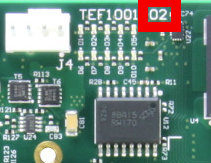
The revision number is shown on the top side of the PCB.
Production Shipment Schedule
This change takes place with immediate effect. If the new revision is not suitable for your application and still the former revision of the board is needed, please contact us.
Contact Information
If you have any questions related to this PCN, please contact Trenz Electronics Technical Support at
- forum.trenz-electronic.de
- wiki.trenz-electronic.de
- support%trenz-electronic.de (subject = PCN-20241121)
phone
national calls: 05741 3200-0
international calls: 0049 5741 3200-0
Disclaimer
Any projected dates in this PCN are based on the most current product information at the time this PCN is being issued, but they may change due to unforeseen circumstances. For the latest schedule and any other information, please contact your local Trenz Electronic sales office, technical support or local distributor.
This PCN follows JEDEC Standard J-STD-046.
Overview
Content Tools