| Company | Trenz Electronic GmbH |
|---|---|
| PCN Number | PCN-20250215 |
| Title | TE0723-03 to TE0723-04 Hardware Revision Change |
| Subject | Hardware Revision Change |
| Issue Date | 2025-06-18 |
Products Affected
This change affects all Trenz Electronic TE0723 SoMs of revision 03: TE0723-03*.
Affected Product | Replacement |
|---|---|
| TE0723-03-11C64-A | TE0723-04-11C68-A (on request) |
| TE0723-03-41C64-A | TE0723-04-41C68-A |
Changes
#1 Changed DCDC EN5311QI (U16, U17, U19, U20) to MPM3834C and adapted power circuit.
Type: Schematic Change
Reason: EOL of Component.
Impact: None. Increased current output capability. Minor changes in electrical characteristics.
#2 Changed power supply architecture.
- Removed diode D5 [REV03].
- Connected 5 V power supply net "VIN" to pin header (J3 pin 8).
- Changed power connection at pin header (J12 pin 1) from power net "5V" to "VIN".
- Added power multiplexer (U9) to switch power supply between primary "VIN" net supply source pin header (J3 pin 8) or pin header (J12 pin 1) and secondary USB connector (J9) supply source.
- Connected DCDC (U16, U20) power good signals via diode D3 to power supervisor (U23) input signal #MR.
- Changed power-up sequencing to following sequence "5V" → "1.0V" → "1.8V" → "1.35V"/"3.3V".
Type: Schematic Change
Reason: Power supply improvement.
Impact: Modified power supply architecture can affect customer board architecture. Verify that new power supply architecture suits with custom application.
#3 Added pin header (J13) assembly option to enable FPGA JTAG only boot mode.
Type: Schematic Change
Reason: QSPI programming problems with newer Vivado versions.
Impact: None. JTAG boot mode directly accessible. Fix QSPI programming problems with newer Vivado versions according to AR#00002 - QSPI Programming issues.
#4 Added pull-up resistor (R96) to connect FTDI chip (U3) signal ADBUS4 with power net "3.3V".
Type: Schematic Change
Reason: Improve JTAG interfacing.
Impact: None.
#5 Added pull-down resistor (R97 ... R99).
Type: Schematic Change
Reason: Avoid floating signals "AMUX_S2", "AMUX_S1", "AMUX_S0".
Impact: Set multiplexer (U10) output channel to channel S1 per default.
#6 Changed flash (U5) from S25FL127SABMFV10 to S25FL128LAGMFI013.
Type: BOM change
Reason: EOL of Component.
Impact: None, no changes in our reference design are expected. JEDEC manufacturer is still the same. Modified device IDs and temperature grade from -40 °C - 105 °C to -40 °C - 85 °C.
#7 Changed analog multiplexer (U10) from CD74HC4051 to TMUX1208QRSVRQ1.
Type: Schematic Change
Reason: EOL of Component.
Impact: None. Minor changes in electrical characteristics.
#8 Changed micro USB connector (J8) from 629105150521 to 629105150921.
Type: Schematic Change
Reason: Follow USB specification.
Impact: Changed micro USB type B receptable to micro USB type AB receptable and mechanical component size.
#9 Changed diode (D1) from BAR43 to MSS2P3-M3/89A.
Type: Schematic Change
Reason: EOL of Component.
Impact: None. Minor changes in electrical characteristics.
#10 Changed resistor (R16) from 1.13 kOhm to 1 kOhm.
Type: Schematic Change
Reason: Follow datasheet recommendation.
Impact: None.
#11 Changed capacitor (C52) from 4.7 µF, 6.3 V to 10 µF, 16 V.
Type: Schematic Change
Reason: BOM optimization
Impact: None. Minor changes in electrical characteristics.
#12 Changed ferrite bead (L1 ... L4, L6 ... L8, L10) from BKP0603HS121-T to MPZ0603S121HT000.
Type: BOM Change
Reason: EOL of component.
Impact: None.
#13 Added additional decoupling capacitors (C64, C65, C70, C73, C76, C94 ... C97, C99, C100, C102 ... C105).
Type: Schematic Change
Reason: Follow AMD recommendation.
Impact: None.
#14 Added additional test points (TP14 ... TP19) to the top side.
Type: Schematic Change
Reason: Improve voltage measurement possibilities.
Impact: None.
#15 Added UKCA- and RoHS-logo.
Type: PCB Change
Reason: Improve product classification.
Impact: None.
Method of Identification
The revision number is printed on the top side of the PCB.
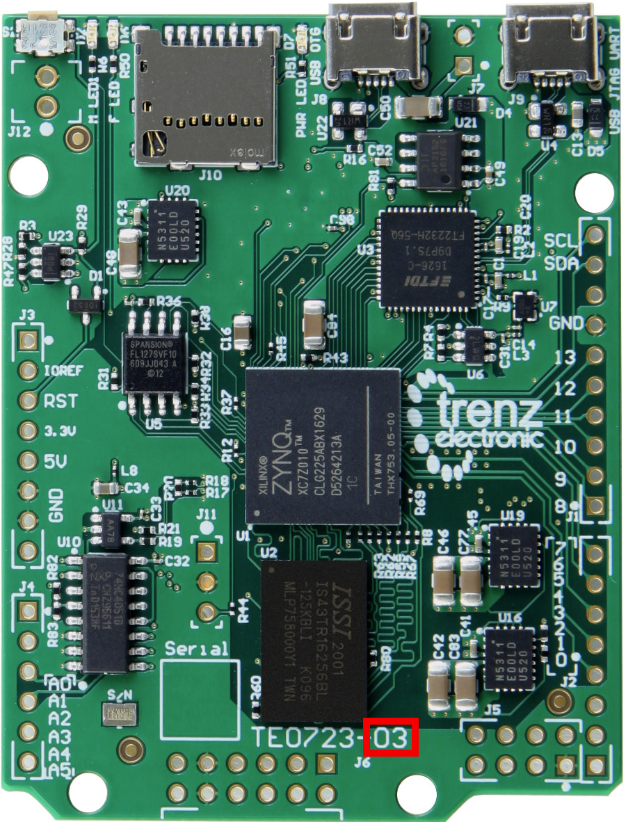
Production Shipment Schedule
From January 2026, after old stock is gone. If the new revision is not suitable for your application and still the former revision of the board is needed, please contact us.
Contact Information
If you have any questions related to this PCN, please contact Trenz Electronics Technical Support at
- forum.trenz-electronic.de
- wiki.trenz-electronic.de
- support%trenz-electronic.de (subject = PCN-20250215)
phone
national calls: 05741 3200-0
international calls: 0049 5741 3200-0
Disclaimer
Any projected dates in this PCN are based on the most current product information at the time this PCN is being issued, but they may change due to unforeseen circumstances. For the latest schedule and any other information, please contact your local Trenz Electronic sales office, technical support or local distributor.
This PCN follows JEDEC Standard J-STD-046.
Overview
Content Tools