| Company | Trenz Electronic GmbH |
|---|---|
| PCN Number | PCN-20250327 |
| Title | TEI0009-02 to TEI0009-03 Hardware Revision Change |
| Subject | Hardware Revision Change |
| Issue Date | 2025-06-10 |
Products Affected
This change affects all Trenz Electronic TEI0009 SoMs: TEI0009-02*.
Affected Product | Changes | Replacement |
|---|---|---|
| TEI0009-02-055-8C | #1, #3, #5 ... #26 | TEI0009-03-PHIQ2A |
| TEI0009-02-055-8CA | #4 ... #25 | TEI0009-03-PHIQ2A |
| TEI0009-02-PHIQ2R | #2, #5 ... #25, #27 | TEI0009-03-PHIQ2A |
Changes
#1 Changed flash IS25LP064A-JBLE (U12) to IS25LP128F-JBLE.
Type: BOM Change
Reason: BOM Optimization.
Impact: Increased memory size. Minor changes in electrical characteristics.
#2 Assembled flash IS25LP064A-JBLE (U12).
Type: BOM Change
Reason: Variant Optimization.
Impact: None. Enable FPGA firmware upgrade possibility. Connected additional SPI flash.
#3 Changed DRAM IS42S16400J-7BL (U10) to IS42S16160J-7BLI.
Type: BOM Change
Reason: BOM Optimization.
Impact: Increased memory size. Minor changes in electrical characteristics. Increased temperature range.
#4 Changed DRAM IS42S16160J-7BL (U10) to IS42S16160J-7BLI.
Type: BOM Change
Reason: BOM Optimization.
Impact: Increased temperature range.
#5 Changed DCDC EN6340QI (U7) to MPM3834CGPA and adapted power circuit.
Type: Schematic Change
Reason: EOL of Component.
Impact: None. Decreased current output capability. Minor changes in electrical characteristics.
#6 Changed DCDC EZ6301QI (U4) to MPM3834CGPA and adapted power circuit.
Type: Schematic Change
Reason: EOL of Component.
Impact: None. Increased current output capability. Minor changes in electrical characteristics. The second channel "2.5V" is realized as a separate component (Change #7).
#7 Added LDO (U13) for "2.5V" voltage rail power supply and adapted power circuit.
Type: Schematic Change
Reason: Change #6.
Impact: None. Power rail "2.5V" LDO (U13) is supplied by power rail "3.3V" instead of power rail "5V" and therefore it is enabled after power rail "3.3V" instead of together with it. Minor changes in electrical characteristics.
#8 Changed input protection range via resistor (R27, R30, R31, R32, R89).
Type: Schematic Change
Reason: Improve input protection.
Impact: None. Minor changes in electrical characteristics.
#9 Changed input power supply jack PJ-002AH-SMT-TR (J12) to 694106106102.
Type: Schematic Change
Reason: Improve power supply handling.
Impact: None. Minor changes in mechanical characteristics.
#10 Changed oscillator 510CCA12M0000CAG12M (U16) to SiT8008BI-73-XXS-12.000000E.
Type: Schematic Change
Reason: BOM Optimization.
Impact: None. Minor changes in electrical characteristics.
#11 Changed oscillator 510CCA25M0000CAG25M (U22) to SiT8008BI-73-XXS-25.000000E.
Type: Schematic Change
Reason: BOM Optimization.
Impact: None. Minor changes in electrical characteristics.
#12 Changed USB 2.0 Micro-B receptable 105017-0001 (J10) to 629105150521.
Type: Schematic Change
Reason: Product improvement.
Impact: None. Minor changes in mechanical characteristics.
#13 Changed diode AOZ8808DI-03 (U6, U8, U11, U23 ... U29, U31 ... U40) to AOZ8S311UD4-03.
Type: Schematic Change
Reason: BOM Optimization.
Impact: None. Minor changes in electrical characteristics.
#14 Added optional configuration flash (U21) alternative assembly option to flash (U5).
Type: Schematic Change
Reason: Increase flexibility for flash usage.
Impact: None.
#15 Added protection fuse (F1), set diode (D12) from not assembled to assembled and added common mode choke (L2) for power supply input.
Type: Schematic Change
Reason: Increase input power supply protection.
Impact: None. Minor changes in electrical characteristics.
#16 Added diode (D18) for USB ESD protection.
Type: Schematic Change
Reason: Increase ESD immunity.
Impact: None. Minor changes in electrical characteristics.
#17 Added pull-up resistor (R87 [REV03]) assembly option (default: not assembled) to #CS signal "AS_nCS" for flash (U5, U21).
Type: Schematic Change
Reason: Increase flash assembly option capability.
Impact: None.
#18 Added pull-up resistor (R88 [REV03]) assembly option (default: not assembled) to #RESET signal "HR_RESET" for HyperRAM (U3).
Type: Schematic Change
Reason: Increase HyperRAM assembly option capability.
Impact: None.
#19 Added pull-up resistor (R82) to #CS signal "HR_CS" for HyperRAM (U3).
Type: Schematic Change
Reason: Use external pull-up resistor.
Impact: None.
#20 Added pull-up resistor for SDRAM signals "CS" (R6 [REV03]), "WE" (R53 [REV03]), "CAS" (R63 [REV03]) and "RAS" (R65 [REV03]).
Type: Schematic Change
Reason: Use external pull-up resistor.
Impact: None.
#21 Added resistor (R101) and capacitor (C37).
Type: Schematic Change
Reason: Increase ESD immunity.
Impact: None.
#22 Changed resistor (R45, R85, R86) from 12 kOhm to 4.02 kOhm.
Type: Schematic Change
Reason: Improve signal integrity.
Impact: None.
#23 Added additional decoupling capacitor (C47 [REV03], C98, C99, C100).
Type: Schematic Change
Reason: Improve power integrity.
Impact: None. Minor changes in electrical characteristics.
#24 Added test point (TP3 ... TP12).
Type: Schematic Change
Reason: Improve voltage measurement possibilities.
Impact: None.
#25 Removed track-it traceability pad completely from PCB.
Type: Schematic Change
Reason: EOL of Component.
Impact: None.
#26 Added PCB spacer (MP1 ... MP4).
Type: Schematic Change
Reason: Improve board handling.
Impact: None.
#27 Assembled DSUB connector (J11).
Type: Schematic Change
Reason: Harmonize variants.
Impact: VGA connector present/usable.
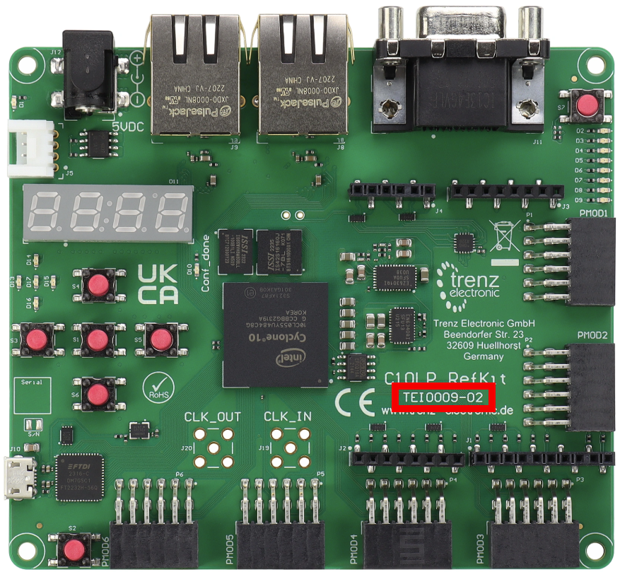
Method of Identification
The revision number is printed on the top side of the PCB.
Production Shipment Schedule
From January 2026, after old stock is gone. If the new revision is not suitable for your application and still the former revision of the board is needed, please contact us.
Contact Information
If you have any questions related to this PCN, please contact Trenz Electronics Technical Support at
- forum.trenz-electronic.de
- wiki.trenz-electronic.de
- support%trenz-electronic.de (subject = PCN-20250327)
phone
national calls: 05741 3200-0
international calls: 0049 5741 3200-0
Disclaimer
Any projected dates in this PCN are based on the most current product information at the time this PCN is being issued, but they may change due to unforeseen circumstances. For the latest schedule and any other information, please contact your local Trenz Electronic sales office, technical support or local distributor.
This PCN follows JEDEC Standard J-STD-046.
Overview
Content Tools