TE0300 has a flexible SPI bus on-board as outlined in the figure below.
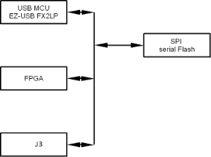
SPI bus topology.
SPI signals on the TE0300 are listed and described in the table below.
name | definition | description |
SPI_Q | serial data output | This output signal is used to transfer data serially out of the device. Data is shifted out on the falling edge of SPI_/C. |
SPI_D | serial data input | This input signal is used to transfer data serially into the device. It receives instructions, addresses, and the data to be programmed. Values are latched on the rising edge of SPI_/C |
SPI_/C | serial clock | This input signal provides the timing of the serial interface. Instructions, addresses, or data present at SPI_D are latched on the rising edge of SPI_/C. Data on SPI_Q changes after the falling edge of SPI_/C. |
SPI_/S | chip select | When this input signal is high, the device is disabled and SPI_Q is at high impedance (Z). |
|
| When this input signal is low, the device is enabled. |
|
| After power-up, a falling edge on SPI_/S is required prior to the start of any instruction to the Flash memory. |
SPI signals summary.
SPI signals are routed to / from bank 2 of the FPGA of the TE0300 is as detailed in the table below.
name | FPGA ball | FPGA pin | J5 pin | J3 pin |
SPI_Q | T4 | IO_L03N_2 | no | see figure below |
SPI_D | N10 | IO_L16N_2 | no | see figure below |
SPI_/C | U16 | IO_L26N_2 | no | see figure below |
SPI_/S | U3 | IO_L01P_2 | no | see figure below |
SPI pin-out summary; SPI signal details (bank 2).
SPI pins on connector J3 cannot be used as GPIOs (general purpose I/Os).
The SPI bus can be used during configuration and operation in a plurality of ways as summarized respectively in Table A (SPI bus for configuration) and Table B (SPI bus for operation).
Any other usage of the SPI bus is neither supported nor recommended.
SPI bus for configuration
The SPI bus is used for configuration in two ways by default:
- EZ-USB â-º Flashthe USB FX2 microcontroller (master) writes the PROM file (containing the FPGA configuration bitstream) to the SPI serial Flash memory (slave)
- FPGA â—„ Flashthe FPGA (master) configures itself in Master SPI mode from the SPI serial Flash memory (slave).
In case (a), the FPGA shall be turned off to release its shared SPI pins.
In case (b), the USB FX2 microcontroller shall three-state (Z = high impedance) its shared SPI pins.
description | usage | EZ-USB FX2LP | FPGA | J3 | serial Flash |
|---|---|---|---|---|---|
EZ-USB â-º Flash | OpenFUT | master | off | deselected | slave |
FPGA â—„ Flash | OpenFUT | inactive | master | deselected | slave |
J3 â-º Flash | custom | inactive | off | master | slave |
Table A: SPI bus modes for configuration.
The PROM file (containing the FPGA configuration bitstream) can be written to the SPI serial Flash memory (slave) also through the SPI pins of J3 (attached device set to master mode). In this case, the FPGA shall be turned off or three-stated to release its shared SPI pins and the USB FX2 microcontroller shall three-state (Z = high impedance) its shared SPI pins.
SPI bus for operation
A plurality of usage combinations of the SPI bus during operation is made available to the user as suggested in Table B below.
description | usage | EZ-USB FX2LP | FPGA | J3 | serial Flash |
EZ-USB â—„â-º Flash | custom | master | off | deselected | slave |
FPGA â—„â-º Flash | custom | inactive | master | deselected | slave |
J3 â—„â-º Flash | custom | inactive | off | master | slave |
EZ-USB â—„â-º J3 | custom | master | off | slave | deselected |
EZ-USB â—„â-º J3 | custom | slave | off | master | deselected |
Table B: SPI bus modes for operation.
Other combinations of master and slave units are neither supported nor recommended.
SPI Header Connector J3
The offset holes of header J3 allow a removable press fit of standard 0.100 inch header pins to connect flying leads without any soldering necessary.
SPI signals are made available on the dedicated header J3 accessible through an SPI programmer with flying leads as described in the table below.
| Signal | J3 pin |
|---|---|
SPI /S |
|
SPI D | |
SPI Q | |
SPI /C | |
GND | |
Vref (3.3 V) | |
|

SPI header (J3).
Overview
Content Tools