USB communication can be performed in one of the following two ways:
- through a USB connector
- through USB lines at one B2B connector
Only one connection type at one time is allowed.
USB Connector
TE0630 is provided with a USB mini-B receptacle (device) connector J1 on the top side.

USB connector (top view).
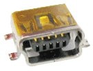
USB mini-B receptacle (device) connector.
The USB cable provides for
- Power supply.
- Configuration by means of the Firmware Upgrade Tool (FUT), recommended for field upgrades. Please use a dedicated JTAG Adapter during development.
- Data communication channel during operation.
USB Pins
USB communication can be performed over 2 pins of B2B connector J5 as detailed in the table below. Ensure resistors R4 and R3 are populated to connect USB B2B pins B2B_D_P and B2B_D_P to USB lines D_P and D_P respectively.
pin number | pin name | signal name | description |
|---|---|---|---|
7 | B2B_D_P | D_P | USB data + (D+) |
9 | B2B_D_N | D_N | USB data - (D-) |
USB pins at B2B connector J5.
TE0630 is equipped with a Cypress EZ-USB FX2 controller to provide a high-speed USB 2.0 interface. The controller uses 4 interfaces (see here):
- USB interface (to USB connector);
- I2C interface (to EEPROM);
- SPI interface (to FPGA and Flash);
- FIFO interface (to FPGA).
The I2C interface connects the USB controller to the EEPROM chip, which stores vendor ID and device ID. See chapter DIP Switch for available options.
The SPI interface id used to communicate with the FPGA and to access the SPI serial Flash chip.
The FIFO interface provides a high-speed communication channel with the FPGA. The interface can transfer up to 48 MB/s burst rate. FPGA pin-out information can be found in the table below.
Signal name | FPGA pin |
|---|---|
FD0 | J6 |
FD1 | H8 |
FD2 | H5 |
FD3 | H6 |
FD4 | G7 |
FD5 | G8 |
FD6 | F8 |
FD7 | A3 |
24MHZ1 | G3 |
PA0/INT0 | D1 |
PA1/INT1 | D2 |
PA2/SLOE | C1 |
PA3/WU | E4 |
PA4/FIFOADDR0 | B1 |
PA5/FIFOADDR1 | C3 |
PA6/PKTEND | B2 |
PA7/FLAGD/SLCS | A2 |
RDY1/SLWR | M3 |
RDY0/SLRD | M4 |
CTL2/FLAGC | E3 |
CTL1/FLAGB | E1 |
CTL0/FLAGA | F3 |
IFCLK | N4 |
USB controller interface: FPGA pin-out
Overview
Content Tools