Host Computer's Software Connection (with I2C EEPROM) Available
The EEPROM switch should be enabled, or these two commands will fail.
Host Computer's Software Connection (with I2C FPGA or other device) Available
General Description
TE USB FX2 module has a flexible IIC (aka I2C) bus on-board as outlined in the figure below.
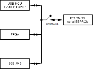
I2C bus topology.
I2C pins on B2B connector J(M)5 cannot be used as GPIOs (general purpose I/Os), as these bus signals are pulled up to 3.3V.
The I2C signals on the TE USB FX2 module are listed and described in the table below
name | definition | description |
|---|---|---|
SDA | serial data | This is a bidirectional pin used to transfer addresses and data into and out of a device. |
SCL | serial clock | This signal is used to synchronize the data transfer to and from a device. |
I2C signals summary.
If the FPGA is set to I2C master mode, it can write to or read from serial EEPROM (always slave mode) and B2B connector J(M)5 (attached device set to slave mode).
If the device attached to the I2C port of B2B J(M)5 connector is set to master mode, it can write to or read from serial EEPROM (always slave mode) and FPGA I2C port (set to slave mode).
The USB FX2 microcontroller can operate just in I2C master mode (default operation). If the user wants to set another device attached to the I2C bus as master device, the USB FX2 microcontroller shall three-state (Z = high impedance) its SCL and SDA pins.
The I2C bus is typically used by the USB FX2 microcontroller to write USB firmware to the serial EEPROM. In this case, the I2C port of the FPGA must be set in slave mode (SCL pin as input), the device attached to the I2C port of B2B J(M)5 connector must be set to slave mode.
Possible I2C operation modes are summarized in the table below.
core | EZ-USB FX2LP | FPGA | B2B J(M)5 | serial EEPROM |
|---|---|---|---|---|
default | master | slave | slave | slave |
custom | inactive | master | slave | slave |
custom | inactive | slave | master | slave |
I2C bus modes summary.
FX2 microcontroller's Interface with the IIC slave device EEPROM: it is used for firmware configuration and firmware loading in RAM from EEPROM
See .
FX2 microcontroller's Interface with IIC slave device FPGA (): in reference design case is used for MB Commands
Pin Name | Pin Name FPGA FPGA Direction | Pin Name FX2 FX2 direction | Description | In the reference design case (1) |
|---|---|---|---|---|
| SDA, SCL and IFCLK are strictly necessary for every standard I2C communication/transaction. They are used in every Logical Architecture Layer or FX2 microcontroller firmware. | ||||
| SDA | SDA Bidirectional | SDA Bidirectional | This pin used to write/read x byte(s) from an y I2C address. | It is used in this two way.
|
| SCL | SCL Input | SCL Output | USB I2C serial clock | USB I2C serial clock |
| IFCLK | IFCLK Input | IFCLK Input | USB 48MHz clock | USB 48MHz clock |
| INT0 is used in I2C transaction between XPS_I2C_SLAVE custom IP block and USB FX2 microcontroller, in reference design (2). | ||||
| INT0 | INT0 Output
| PA0 Input
| Pin value is rised by FPGA to request the execution of a service routine (an ISR or a polling) by USB FX2 μC should | If XPS_I2C_SLAVE custom IP block and a is used,
When the FX2 microcontroller's firmware read the rise of pin INT0 |
| INT1 is NOT is used in I2C transaction between XPS_I2C_SLAVE custom IP block and USB FX2 microcontroller, in reference design (2). | ||||
| INT1 | INT1 Input
| PA1 Output
| Pin value is rised by USB FX2 µC to request the execution of | NOT USED FOR I2C transaction: the interrupt (to MicroBlaze) used |
Description of FPGA IIC Interface with FX2 microcontroller
(1) Reference design: Logical Architecture Layer = Reference Architecture Layer and FX2 firmware= Reference FX2 firmware
(2) MB Commands require the XPS_I2C_SLAVE custom IP block and a proper FX2 interrupt handler (i2c_slave_int_handler() function in interrupt.c) running on MicroBlaze.
MB Commands require the XPS_I2C_SLAVE custom IP block and a proper FX2 interrupt handler (i2c_slave_int_handler() function in interrupt.c running on MicroBlaze); the FX2 interrupt handler is called to handle the signal interrupt xps_i2c_slave_0_IP2INTC_Irpt. The i2c_slave_int_handler() function actually execute the I2C delivered MB Command; when MicroBlaze's software wants to send information to the host computer (through USB FX2 microcontroller), it should write MB2FX2_REGs of XPS_I2C_SLAVE custom IP block. The IP block will rise (USB_INT => INT0) pin INT0 output as a flag. The FX2 microcontroller will manage this flag indication (INT0=1 => FPGA_INT0=1); after this, the FX2 microcontroller could read the registers (MB2FX2_REGs) of XPS_I2C_SLAVE custom IP block.
Overview
Content Tools