Page History
...
| Name / opt. VHD Name | Direction | Pin | Bank Power | Description |
|---|---|---|---|---|
| BOOTSEL2 | out | L10 | +3.3V | HPS boot select pin 2 |
| CPU_GPIO_0 | in | N10 | +3.3V | Voltage selection via software for FMC_VADJ (U43 → VS0 pin) |
| CPU_GPIO_1 | in | N9 | +3.3V | Voltage selection via software for FMC_VADJ (U43 → VS1 pin) |
| CPU_GPIO_2 | in | N11 | +3.3V | Voltage selection via software for FMC_VADJ (U43 → VS2 pin) |
| CPU_GPIO_3 | in | L1 | +3.3V | FMC power enable control via software |
| CPU_GPIO_4 | in | H4 | +3.3V | Fan control via software |
| BDBUS0 | in | D1 | +3.3V_MAX10 | FTDI UART TXD pin |
| BDBUS1 | out | C1 | +3.3V_MAX10 | FTDI UART RXD pin |
| EN_0V9 | out | F1 | +3.3V_MAX10 | +0.9V power enable |
| EN_1V8 | out | D12 | +3.3V_MAX10 | +1.8V power enable |
| EN_2V5 | out | A12 | +3.3V_MAX10 | +2.5V power enable |
| EN_3V3 | out | B13 | +3.3V_MAX10 | +3.3V power enable |
| EN_5V0 | out | A7 | +3.3V_MAX10 | +5.0V power enable |
| EN_DDR_FPGA | out | E13 | +3.3V_MAX10 | FPGA DDR power enable |
| EN_DDR_HPS | out | F13 | +3.3V_MAX10 | HPS DDR power enable |
| EN_FMC | out | E1 | +3.3V_MAX10 | FMC_VADJ power enable |
| EN_FMC_3V3 | out | C13 | +3.3V_MAX10 | +3.3V FMC power enable |
| EN_FMC_12V | out | C12 | +3.3V_MAX10 | +12.0V FMC power enable |
| EN_VCC | out | A10 | +3.3V_MAX10 | VCC power enable |
| FAN_EN | out | D13 | +3.3V_MAX10 | Fan control |
| FMC_PG_C2M | out | K7 | +3.3V | FMC power good signal to FMC connector |
| FMC_PRSNT_M2Cn | in | J7 | +3.3V | FMC card detection from FMC connector / currently_not_used |
| FPGA_GPIO_0 | out | K11 | VDD_DDR_FPGA | FPGA IO (FPGA pin AG10) / FPGA UART RXD |
| FPGA_GPIO_1 | in | J10 | VDD_DDR_FPGA | FPGA IO (FPGA pin AH9) / FPGA UART TXD |
| FPGA_RSTn | out | L13 | VDD_DDR_FPGA | FPGA reset |
| FPGA_RSTn_SW | in | B4 | +3.3V_MAX10 | FPGA reset button |
| FMC_TCK | out | M8 | +3.3V | FMC JTAG TCK |
| FMC_TDI | out | M9 | +3.3V | FMC JTAG TDI |
| FMC_TDO | in | M10 | +3.3V | FMC JTAG TDO |
| FMC_TMS | out | M11 | +3.3V | FMC JTAG TMS |
| FPGA_TCK | out | K2 | +3.3V | HPS JTAG TCK |
| FPGA_TDI | out | J1 | +3.3V | FPGA JTAG TDI |
| FPGA_TDO | in | L2 | +3.3V | FPGA JTAG TDO |
| FPGA_TMS | out | J2 | +3.3V | FPGA JTAG TMS |
| FTDI_JTAG_TCK | in | G2 | +3.3V_MAX10 | FTDI JTAG TCK |
| FTDI_JTAG_TDI | in | F5 | +3.3V_MAX10 | FTDI JTAG TDI |
| FTDI_JTAG_TDO | out | F6 | +3.3V_MAX10 | FTDI JTAG TDO |
| FTDI_JTAG_TMS | in | G1 | +3.3V_MAX10 | FTDI JTAG TMS |
| HPS_TCK | out | K1 | +3.3V | HPS JTAG TCK |
| HPS_TDI | out | M4 | +3.3V | HPS JTAG TDI |
| HPS_TDO | in | J6 | +3.3V | HPS JTAG TDO |
| HPS_TMS | out | M7 | +3.3V | HPS JTAG TMS |
| HPS_RSTn | out | L11 | +3.3V | HPS reset |
| HPS_RSTn_BO | in | K6 | +3.3V | Brown Out detection |
| HPS_RSTn_SW | in | J5 | +3.3V | Reset button |
| HPS_WARM_RSTn | out | M3 | +3.3V | HPS warm reset |
| HPS_WARM_RSTn_SW | in | K5 | +3.3V | HPS warm reset button |
| JTAGSEL0 | in | F9 | +3.3V_MAX10 | Select JTAG connection |
| JTAGSEL1 | in | E9 | +3.3V_MAX10 | Select JTAG connection |
| LED_1V8 | out | H2 | +3.3V_MAX10 | +1.8V power led |
| LED_FMC_VADJ | out | C9 | +3.3V_MAX10 | FMC_VADJ power good led |
| LED_VCC | out | F12 | +3.3V_MAX10 | VCC power good led |
| LED_VDD_DDR_FPGA | out | E6 | +3.3V_MAX10 | FPGA DDR VDD power good led |
| LED_VDD_DDR_HPS | out | H3 | +3.3V_MAX10 | HPS DDR VDD power good led |
| LED_VTT_DDR_FPGA | out | D6 | +3.3V_MAX10 | FPGA DDR VTT power good led |
| LED_VTT_DDR_HPS | out | G4 | +3.3V_MAX10 | HPS DDR VTT power good led |
| MODE | out | A11 | +3.3V_MAX10 | +5.0V voltage regulator mode selection |
| MODE_DDR_FPGA | out | E10 | +3.3V_MAX10 | Voltage regulator mode selection for FPGA DDR power |
| MODE_DDR_HPS | out | F10 | +3.3V_MAX10 | Voltage regulator mode selection for HPS DDR power |
| MODE_VCC | out | D9 | +3.3V_MAX10 | VCC voltage regulator mode selection |
| MSEL0 | out | N5 | +3.3V | Configuration mode selection pin 0 |
| MSEL1 | out | N3 | +3.3V | Configuration mode selection pin 1 |
| MSEL2 | out | N2 | +3.3V | Configuration mode selection pin 2 |
| MSEL3 | out | N4 | +3.3V | Configuration mode selection pin 3 |
| MSEL4 | out | N6 | +3.3V | Configuration mode selection pin 4 |
| PG_1V8 | in | D11 | +3.3V_MAX10 | +1.8V power good signal |
| PG_2V5 | in | C11 | +3.3V_MAX10 | +2.5V power good signal |
| PG_3V3 | in | B12 | +3.3V_MAX10 | +3.3V power good signal |
| PG_5V0 | in | A8 | +3.3V_MAX10 | +5.0V power good signal |
| PG_VCC | in | B11 | +3.3V_MAX10 | VCC power good signal |
| PG_VDD_FPGA | in | E12 | +3.3V_MAX10 | FPGA VDD DDR power good signal |
| PG_VDD_HPS | in | G10 | +3.3V_MAX10 | HPS VDD DDR power good signal |
| PG_VTT_FPGA | in | B10 | +3.3V_MAX10 | FPGA VTT DDR power good signal |
| PG_VTT_HPS | in | B5 | +3.3V_MAX10 | HPS VTT DDR power good signal |
| POK_FMC | in | E3 | +3.3V_MAX10 | FMC_VADJ power good signal |
| PWR_SEL | out | E4 | +3.3V_MAX10 | Power selection pin for FMC_VCCPD voltage at U37 (Cyclone V - Bank 8A VCCPD voltage) |
| PWR_SWT_EN | out | C10 | +3.3V_MAX10 | Power enable pin for FMC_VCCPD voltage at U37 |
| USER_BTN_FPGA | out | G12 | VDD_DDR_FPGA | FPGA user button pin |
| USER_BTN_SW | in | B3 | +3.3V_MAX10 | user button |
| VID0_SW | in | F8 | +3.3V_MAX10 | Dip switch S8A for FMC_VADJ voltage selection |
| VID1_SW | in | E8 | +3.3V_MAX10 | Dip switch S8B for FMC_VADJ voltage selection |
| VID2_SW | in | D8 | +3.3V_MAX10 | Dip switch S8C for FMC_VADJ voltage selection |
| VID0 | out | B2 | +3.3V_MAX10 | Voltage selection pin 0 (VS0) for FMC_VADJ voltage at U43 |
| VID1 | out | C2 | +3.3V_MAX10 | Voltage selection pin 1 (VS0VS1) for FMC_VADJ voltage at U43 |
| VID2 | out | F4 | +3.3V_MAX10 | Voltage selection pin 2 (VS0VS2) for FMC_VADJ voltage at U43 |
| JTAGEN | in | E5 | +3.3V_MAX10 | enable/disable JTAG access to system controller MAX10 |
| BDBUS2 | - | B1 | +3.3V_MAX10 | / currently_not_used |
| BDBUS3 | - | A2 | +3.3V_MAX10 | / currently_not_used |
| BDBUS4 | - | A3 | +3.3V_MAX10 | / currently_not_used |
| BDBUS5 | - | A4 | +3.3V_MAX10 | / currently_not_used |
| BDBUS6 | - | A5 | +3.3V_MAX10 | / currently_not_used |
| BDBUS7 | - | A6 | +3.3V_MAX10 | / currently_not_used |
| CLK_MAX10 | - | H6 | +3.3V | SI5338A → CLK2A pin / currently_not_used |
| CLKSEL0 | - | N8 | +3.3V | Cyclone V clock select pin 0 / currently_not_used |
| CLKSEL1 | - | N7 | +3.3V | Cyclone V clock select pin 1 / currently_not_used |
| CONF_DONE_I | - | L5 | +3.3V | Cyclone V CONF_DONE pin / currently_not_used |
| DEVCLRn | - | B9 | +3.3V_MAX10 | Device-wide reset for MAX 10 / currently_not_used |
| ETH_RST | - | G5 | +3.3V | Ethernet phy reset / currently_not_used |
| FMC_SCL | - | N12 | +3.3V | FMC I²C interface / currently_not_used |
| FMC_SDA | - | M13 | +3.3V | FMC I²C interface / currently_not_used |
| FMC_TRST# | - | M12 | +3.3V | FMC JTAG test reset / currently_not_used |
| FPGA_GPIO_2 | - | K12 | VDD_DDR_FPGA | FPGA IO (FPGA pin AF11) / currently_not_used |
| FPGA_GPIO_3 | - | L12 | VDD_DDR_FPGA | FPGA IO (FPGA pin AG11) / currently_not_used |
| FPGA_GPIO_4 | - | G13 | VDD_DDR_FPGA | FPGA IO (FPGA pin AA13) / currently_not_used |
| FPGA_GPIO_5 | - | H13 | VDD_DDR_FPGA | FPGA IO (FPGA pin AB13) / currently_not_used |
| FPGA_GPIO_6 | - | H8 | VDD_DDR_FPGA | FPGA IO (FPGA pin AK2) / currently_not_used |
| FPGA_GPIO_7 | - | H9 | VDD_DDR_FPGA | FPGA IO (FPGA pin AK3) / currently_not_used |
| FPGA_GPIO_8 | - | J9 | VDD_DDR_FPGA | FPGA IO (FPGA pin AJ4) / currently_not_used |
| FPGA_GPIO_9 | - | K10 | VDD_DDR_FPGA | FPGA IO (FPGA pin AK4) / currently_not_used |
| FPGA_GPIO_10 | - | J13 | VDD_DDR_FPGA | FPGA IO (FPGA pin AE13) / currently_not_used |
| FPGA_GPIO_11 | - | J12 | VDD_DDR_FPGA | FPGA IO (FPGA pin AF13) / currently_not_used |
| FPGA_GPIO_12 | - | H10 | VDD_DDR_FPGA | FPGA IO (FPGA pin AD14) / currently_not_used |
| HPS_SPI_SS/BOOTSEL0 | - | K8 | +3.3V | HPS boot select pin 0 / currently_not_used |
| HPS_TRST# | - | M5 | +3.3V | HPS JTAG test reset / currently_not_used |
| nCONFIG_I | - | M1 | +3.3V | Cyclone V nCONFIG pin / currently_not_used |
| nSTATUS_I | - | L4 | +3.3V | Cyclone V nSTATUS pin/ currently_not_used |
| QSPI_CS/BOOTSEL1 | - | J8 | +3.3V | HPS boot select pin 1 / currently_not_used |
| STATUS | - | H1 | +3.3V_MAX10 | status led / currently_not_used |
| USB_HUB_RST | - | L3 | +3.3V | USB hub (U33) reset / currently_not_used |
| USB_RST | - | H5 | +3.3V | USB phy (U8) reset / currently_not_used |
| USER_BTN_HPS | - | M2 | +3.3V | HPS user button pin / currently_not_used |
Functional Description
DCDC Mode Control
The mode signals are connected to "1".
...
MODE_DCDC_VCC,
MODE_DCDC_5V
...
1
...
MODE_DCDC_FPGA,
MODE_DCDC_HPS
...
Fan control
Can be enabled/disabled through the Intel Cyclone V HPS "CPU_GPIO_4" pin.
JTAG control
The FTDI JTAG is connected to the Intel MAX 10, the Intel Cyclone V HPS and Fabric and to the FMC Connector according to the following table.
| JTAGSEL0 | JTAGSEL1 | JTAGEN | JTAG selection |
|---|---|---|---|
| X | X | 1 - (ON) | Intel MAX 10 |
| 0 - (ON) | 0 - (ON) | 0 - (OFF) | Cyclone V HPS |
| 0 - (ON) | 1 - (OFF) | 0 - (OFF) | Cyclone V FPGA |
| 1 - (OFF) | 0 - (ON) | 0 - (OFF) | FMC |
LED Control
The leds signals their power good status.
UART
UART signal are routed directly from FTDI chip through Intel MAX 10 to Cyclone V FPGA.
| FTDI FT2232H-56Q | Direction | Cyclone V FPGA |
|---|---|---|
| BDBUS0 (TXD) | → | FPGA_GPIO_0 (RXD, Pin AG10) |
| BDBUS1 (RXD) | ← | FPGA_GPIO_1 (TXD, Pin AH9) |
User button
The user button is connected to the USER_BTN_FPGA pin AB21 from Cyclone V FPGA.
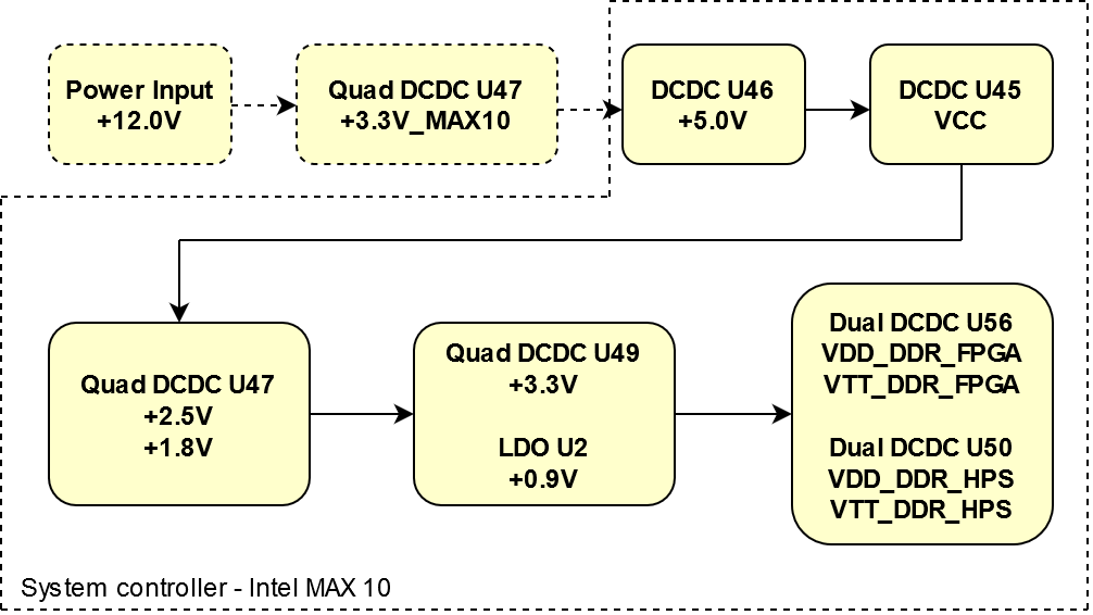
Power management
The power sequencing is
Fan Control
Can be enabled/disabled through the Intel Cyclone V HPS "CPU_GPIO4".
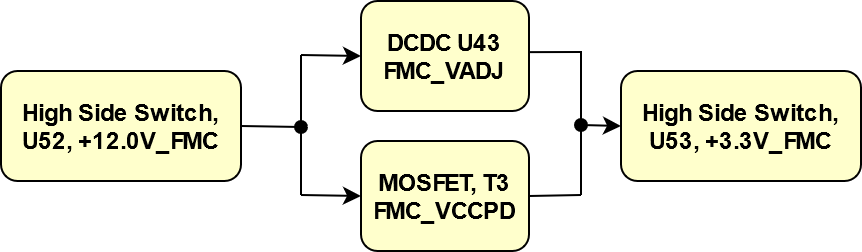
FMC Voltage Control
The power is enabled if signal "CPU_GPIO3" is set to "1" and there is an FMC card. Then, the +12.0 V level is enabled. After that, the adjustable voltage is enabled. Finally, the +3.3 V level is enabled. Then, the signal "FMC_PG_C2M" is asserted.
JTAG Control
The FTDI JTAG is connected to the Intel MAX10, the Intel Cyclone V HPS and Fabric and to the FMC Connector according to the following table.
...
LED Control
The leds signals their power good status.
UART
The second channel of the JTAG FTDI interface delievers an UART connection to the Intel Cyclone V fabric.
User Button
The User Button is connected to the FPGA.
Power Management
The power sequencing is handled inside the system controller according to the next figure, starting with DCDC U46 +5.0V.
| Scroll Title | ||||||||||||||||||||||||||||||||||||||||||||||||||||||||||||||||
|---|---|---|---|---|---|---|---|---|---|---|---|---|---|---|---|---|---|---|---|---|---|---|---|---|---|---|---|---|---|---|---|---|---|---|---|---|---|---|---|---|---|---|---|---|---|---|---|---|---|---|---|---|---|---|---|---|---|---|---|---|---|---|---|---|
| ||||||||||||||||||||||||||||||||||||||||||||||||||||||||||||||||
|
The FMC power sequencing depends on the assertion through the signals "CPU_GPIO3" and "FMC_PRSNT_M2Cn". If both of them are asserted, the +12.0 V level starts, followed by the adjustabel voltage level with the according pre-driver voltage and finally, the +3.3 V level is started.
Voltage regulator mode control
| Designator | Signal | State | Description |
|---|---|---|---|
| U45 | MODE_VCC | 1 | Forced continous mode |
| U46 | MODE | 1 | Forced continous mode |
| U56 | MODE_DDR_FPGA | 1 | Pulse-skipping mode for VDD |
| U50 | MODE_DDR_HPS | 1 | Pulse-skipping mode for VDD |
For more information about possible modes see datasheet of voltage regulators.
FMC power control
The FMC adjustable voltage selection FMC_VADJ (U43) can be done by the dip switches VID0_SW (S8A), VID1_SW (S8B) and VID2_SW (S8C) or by the Intel Cyclone V HPS via CPU_GPIO_0 pin, CPU_GPIO_1 pin and CPU_GPIO_2 pin. The choice is done according to the next table.
VID2_SW (S8C)/ CPU_GPIO_2 | VID1_SW (S8B)/ CPU_GPIO_1 | VID0_SW (S8A)/ CPU_GPIO_0 | Voltage | Notes |
|---|---|---|---|---|
| ON / 0 | ON / 0 | ON / 0 | 3.3V | - |
| ON / 0 | ON / 0 | OFF / 1 | 2.5V | - |
| ON / 0 | OFF / 1 | ON / 0 | 1.8V | - |
| ON / 0 | OFF / 1 | OFF / 1 | 1.5V | - |
| OFF / 1 | ON / 0 | ON / 0 | 1.25V | - |
| OFF / 1 | ON / 0 | OFF / 1 | 1.2V | - |
| OFF / 1 | OFF / 1 | ON / 0 | 0.8V | not supported by Intel Cyclone V |
| OFF | OFF | OFF | CPU-dependent | select voltages with CPU_GPIO_* pins |
The FMC power can be enabled or disabled via software with CPU_GPIO_3 pin, when the dip switches VID0_SW (S8A), VID1_SW (S8B) and VID2_SW (S8C) are set to OFF. If the FMC_VADJ voltage is selected by the dip switches, FMC power is always enabled.
The FMC power sequencing is handled as shown in the next figure.
| Scroll Title | ||||||||||||||||||||||||||||||||||||||||||||||||||||||||||||||||
|---|---|---|---|---|---|---|---|---|---|---|---|---|---|---|---|---|---|---|---|---|---|---|---|---|---|---|---|---|---|---|---|---|---|---|---|---|---|---|---|---|---|---|---|---|---|---|---|---|---|---|---|---|---|---|---|---|---|---|---|---|---|---|---|---|
| ||||||||||||||||||||||||||||||||||||||||||||||||||||||||||||||||
| ||||||||||||||||||||||||||||||||||||||||||||||||||||||||||||||||
| Scroll Title | ||||||||||||||||||||||||||||||||||||||||||||||||||||||||||||||||
| ||||||||||||||||||||||||||||||||||||||||||||||||||||||||||||||||
|

The FMC adjustable voltage selection can be done manually by the switches or automatically by the Intel Cyclone V HPS. The choice is done via the switches according to the next table. The voltage for the Intel Cyclone V HPS pre-driver is selected according to the voltage setting.
...
Reset Management
...
|
Reset Management
The reset buttons are connected via the system controller to the according reset locations.
| Designator | Name | connected to | Notes |
|---|---|---|---|
| S1 | HPS_RSTn_SW | HPS_RSTn | Button |
| U54 | HPS_RSTn_BO | HPS_RSTn | Brown out detection |
| S3 | HPS_WARM_RSTn_SW | HPS_WARM_RSTn | Button |
| S4 | FPGA_RSTn_SW | FPGA_RSTn | Button |
Configuration sheme control
| MSEL4 | MSEL3 | MSEL2 | MSEL1 | MSEL0 | Configuration sheme |
|---|---|---|---|---|---|
| 0 | 0 | 0 | 1 | 0 | FPP x16 Fast, compression feature enabled |
Appx. A: Change History and Legal Notices
Revision Changes
SC REV02 to REV03
- bugfixes
- add configuration sheme
SC CPLD REV01 to REV02
- Changed pin connections
- Changed JTAG connection
- Changed reset connection
- Changed FMC Vadj Voltage selection
- Changed power sequencing
...
| Date | Document Revision | CPLD Firmware Revision | Supported PCB Revision | Authors | Description | ||||||||||||||||||||||
|---|---|---|---|---|---|---|---|---|---|---|---|---|---|---|---|---|---|---|---|---|---|---|---|---|---|---|---|
|
| REV03 | REV02 |
| Work in progressRevision 03 release | ||||||||||||||||||||||
| 2020-02-19 | v.197 | REV02 | REV02 |
| Initial release | ||||||||||||||||||||||
| All |
|
...
Overview
Content Tools