...
- SoC/FPGA
- Package: SFVC784
- Device: ZU2EG, ZU3EG, ZU4EG, ZU5EGZU2 ...ZU5, *
- Engine: G (General Purpose) EG, CG, EV, *
- Speed: -1 (slowest), -1L, -2, -2L, 3, *, **
- Temperature: I, E, *, **Temperature: Industrial (-40 ~ 85 °C)
- RAM/Storage
- 2 GByte 2x DDR4 SDRAM, 32-Bit databus-width
- Data Width: 16 Bit
- Size: 8 Gb, *
- Speed: 2400 Mbps, ***
- 2x 128 MByte QSPI boot Flash in dual parallel mode
- Data Width: 8 Bit
- Size: 512 Mb Gb, *
- 1x e.MMC Memory
- Data Width: 16 Bit
- Size: 8 Gb, *
8 GByte e.MMC Memory (up to 64 GByte) - MAC address serial EEPROM with EUI-48 node identity
- On Board
- Graphic Processing Unit (GPU) :Mali-400 MP2
- Lattice MachXO2 CPLD
- Programmable Clock Generator
- Hi-speed USB2 ULPI Transceiver
- 4x LEDS
- InterfaceInterface
- Power
- All power supplies regulators on board
- Dimension
- Note
- * depends on assembly version
- ** also non low power assembly options possible
- *** depends on used U+ Zynq and DDR4 combination
- Rugged for shock and high vibration
Block Diagram
| Page properties |
|---|
|
add drawIO object here.
|
...
| Scroll Title |
|---|
| anchor | Figure_OV_MC |
|---|
| title | TE0821 main components |
|---|
|
| Scroll Ignore |
|---|
| draw.io Diagram |
|---|
| border | false |
|---|
| |
|---|
| diagramName | TE0821_OV_MC |
|---|
| simpleViewer | false |
|---|
| width | |
|---|
| links | auto |
|---|
| tbstyle | hidden |
|---|
| diagramDisplayName | |
|---|
| lbox | true |
|---|
| diagramWidth | 641 |
|---|
| revision | 89 |
|---|
|
|
| Scroll Only |
|---|
|
|
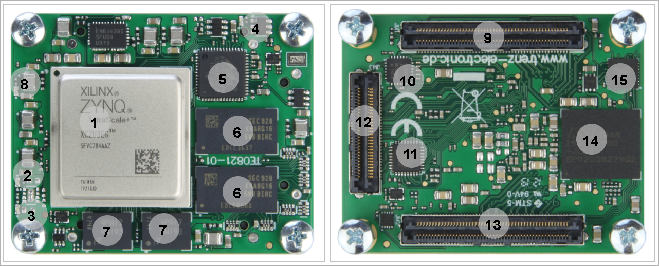
- Xilinx Zynq UltraScale+ XCZU3EG, U1
- Red LED (ERR_OUT), D3
- Green LED (ERR_STATUS), D4
- Red LED (DONE), D1
- 10/100/1000 Mbps energy efficient ethernet transceiver, U8
- 8Gb DDR4, U2-U3
- 512 Mbit QSPI flash memory, U7-U17
- Green User LED, D2
- B2B connector Samtec Razor Beam, JM1
- Programmable clock generator, U10
- USB2.0 Transceiver, U18
- B2B connector Samtec Razor Beam, JM3
- B2B connector Samtec Razor Beam, JM2
- 8 GByte eMMC memory, U6
- Lattice Semiconductor MachXO2 System Controller CPLD, U21
...
| Scroll Title |
|---|
| anchor | Table_OV_IDS |
|---|
| title | Initial delivery state of programmable devices on the module |
|---|
|
| Scroll Table Layout |
|---|
| orientation | portrait |
|---|
| sortDirection | ASC |
|---|
| repeatTableHeaders | default |
|---|
| style | |
|---|
| widths | |
|---|
| sortByColumn | 1 |
|---|
| sortEnabled | false |
|---|
| cellHighlighting | true |
|---|
|
Storage device name | Content | Notes |
|---|
Dual QSPI Flash Memory | Not programmed |
| eMMC Memory | Not programmed |
| | Programmable Clock Generator | Not programmed |
| | CPLD (LCMXO2-256HC) | ???? FirmwareProgrammed | TE0821 CPLD |
|
Configuration Signals
...
| Scroll Title |
|---|
| anchor | Table_OV_BP |
|---|
| title | Boot process. |
|---|
|
| Scroll Table Layout |
|---|
| orientation | portrait |
|---|
| sortDirection | ASC |
|---|
| repeatTableHeaders | default |
|---|
| style | |
|---|
| widths | |
|---|
| sortByColumn | 1 |
|---|
| sortEnabled | false |
|---|
| cellHighlighting | true |
|---|
|
MODE Pin | Boot Mode |
|---|
| Low | QSPI | | High | SD Card |
|
Please refer to the TE0821 CPLD.
| Scroll Title |
|---|
| anchor | Table_OV_RST |
|---|
| title | Reset process. |
|---|
|
| Scroll Table Layout |
|---|
| orientation | portrait |
|---|
| sortDirection | ASC |
|---|
| repeatTableHeaders | default |
|---|
| style | |
|---|
| widths | |
|---|
| sortByColumn | 1 |
|---|
| sortEnabled | false |
|---|
| cellHighlighting | true |
|---|
|
Signal | B2B | I/O | Note |
|---|
EN | JM1-28 | Input | CPLD Enable Pin |
|
...
Signals, Interfaces and Pins
...
| Scroll Title |
|---|
| anchor | Table_PWR_PR |
|---|
| title | Module power rails. |
|---|
|
| Scroll Table Layout |
|---|
| orientation | portrait |
|---|
| sortDirection | ASC |
|---|
| repeatTableHeaders | default |
|---|
| style | |
|---|
| widths | |
|---|
| sortByColumn | 1 |
|---|
| sortEnabled | false |
|---|
| cellHighlighting | true |
|---|
|
| Power Rail Name | B2B JM1 Pin | B2B JM2 Pin | B2B JM3 Pin | Direction | Notes |
|---|
| VIN | 1, 3, 5 | 2, 4, 6, 8 | - | Input | Supply voltage from the carrier board | | 3.3V | - | 10, 12 | - | Output | Internal 3.3V voltage level | | VCCO_HD25_26 | 9,11 |
| - | Input | 0 to 3.3V Voltage | | 3.3VIN | 13, 15 | - | - | Input | Supply voltage from the carrier board | | 1.8V | 39 | - | - | Output | Internal 1.8V voltage level | | JTAG VREF | - | 91 | - | Output | JTAG reference voltage.
Attention: Net name on schematic is "3.3VIN" | | VCCO_HD24_ |
64High performance I/O bank voltage| 0 to 3.3V Voltage | | VCCO_65 | - | 5 |
Input | High performance I/O bank voltage | | - | Input | 0 to 1.8V Voltage | | PSBATT | 79 | - |
VCCO_66 | 9, 11High performance I/O bank voltage
|
Bank Voltages
| Scroll Title |
|---|
| anchor | Table_PWR_BV |
|---|
| title | Zynq SoC bank voltages. |
|---|
|
| Scroll Table Layout |
|---|
| orientation | portrait |
|---|
| sortDirection | ASC |
|---|
| repeatTableHeaders | default |
|---|
| style | |
|---|
| widths | |
|---|
| sortByColumn | 1 |
|---|
| sortEnabled | false |
|---|
| cellHighlighting | true |
|---|
|
| FPGA Bank | Schematic | Voltage | Note |
|---|
| Bank 24 HD | VCCO_HD24_24 | Variable | Max voltage 3.3V | | Bank 25 HD |
| Variable | Max voltage 3.3V | | Bank 26 HD | VCCO_HD25_26 | Variable | Max voltage 3.3V | | Bank 44 HD | VCCO_HD24_44 | Variable | Max voltage 3.3V | | Bank 64 HP | VCCO_64 | N.C | Not Connected | | Bank 65 HP | VCCO_65 | Variable | Max voltage 1.8V | | Bank 66 HP | VCCO_66 | 1.8V |
| | Bank 500 PSMIO | VCCO_PSIO0_500 | 1.8V |
| Bank 501 PSMIO | VCCO_PSIO1_501 | 3.3V |
| | Bank 502 PSMIO | VCCO_PSIO2_502 | 1.8V |
| | Bank 503 PSCONFIG | VCCO_PSIO3_503 | 1.8V |
| | Bank 504 PSDDR | DDR_1V2 | 1.2V |
|
|
...
| Scroll Title |
|---|
| anchor | Table_TS_AMR |
|---|
| title | PS absolute maximum ratings |
|---|
|
| Scroll Table Layout |
|---|
| orientation | portrait |
|---|
| sortDirection | ASC |
|---|
| repeatTableHeaders | default |
|---|
| style | |
|---|
| widths | |
|---|
| sortByColumn | 1 |
|---|
| sortEnabled | false |
|---|
| cellHighlighting | true |
|---|
|
| Description | Min | Max | Unit | Notes |
|---|
VIN supply voltage | -0.3 | 7 | V | See EN6347QI and TPS82085SIL datasheets3.3VIN supply | | 3.3VIN supply voltage | -0.1 | 3.630 | V | Xilinx DS925 and TPS27082L datasheet | | PS I/O supply voltage, VCCO_PSIO | -0.5 | 3.630 | V | Xilinx document DS925 | | PS I/O input voltage | -0. | 13.6305 | VCCO_PSIO + 0.55 | V | Xilinx document DS925 | | HP | DS925 and TPS27082L datasheetPS I/O bank supply voltage, VCCO | _PSIO | -0.5 | 32. | 6300 | V | Xilinx document DS925 | PS | HP I/O bank input voltage | -0. | 555 | VCCO | _PSIO + 0.55 | V | Xilinx document DS925HP | | HD I/O bank supply voltage, VCCO | -0.5 | 23. | 04 | V | Xilinx document DS925 | HP | HD I/O bank input voltage | -0.55 | VCCO + 0.55 | V | Xilinx document DS925 | | PS GTR reference clocks absolute input voltage | -0.5 | 1.1 | V | Xilinx document DS925 | | PS GTR absolute input voltage | -0.5 | 1.1 | V | Xilinx document DS925 | Voltage on SC CPLD pins | -0.5 | 3.75 | V | Lattice Semiconductor MachXO2 datasheet | Storage temperature | -40 | +85 | °C | See eMMC datasheet |
|
...
| Scroll Title |
|---|
| anchor | Table_TS_ROC |
|---|
| title | Recommended operating conditions. |
|---|
|
| Scroll Table Layout |
|---|
| orientation | portrait |
|---|
| sortDirection | ASC |
|---|
| repeatTableHeaders | default |
|---|
| style | |
|---|
| widths | |
|---|
| sortByColumn | 1 |
|---|
| sortEnabled | false |
|---|
| cellHighlighting | true |
|---|
|
| Parameter | Min | Max | Units | Reference Document |
|---|
| VIN supply voltage | 3.3 | 6 | V | See TPS82085S datasheet | | 3.3VIN supply voltage | 3.3 | 3.465 | V | See LCMXO2-256HC, Xilinx DS925 datasheet | | PS I/O supply voltage, VCCO_PSIO | 1.710 | 3.465 | V | Xilinx document DS925 | | PS I/O input voltage | –0.20 | VCCO_PSIO + 0.20 | V | Xilinx document DS925 | | HP I/O banks supply voltage, VCCO | 0.950 | 1.9 | V | Xilinx document DS925 | | HP I/O banks input voltage | -0.20 | VCCO + 0.20 | V | Xilinx document DS925 | | HD I/O banks supply voltage, VCCO | 1.14 | 3.4 | V | Xilinx document DS925 | | HD I/O banks input voltage | -0.20 | VCCO + 0.20 | V | Xilinx document DS925 | | Voltage on SC CPLD pins | -0.3 | 3.6 | V | Lattice Semiconductor MachXO2 datasheet | | Operating Temperature Range | 0 | 85 | °C | Xilinx document DS925, extended grade Zynq temperarure range |
|
...