...
| Scroll Title |
|---|
| anchor | Table_SIP_B2B |
|---|
| title | General PL I/O to B2B connectors information |
|---|
|
| Scroll Table Layout |
|---|
| orientation | portrait |
|---|
| sortDirection | ASC |
|---|
| repeatTableHeaders | default |
|---|
| style | |
|---|
| widths | |
|---|
| sortByColumn | 1 |
|---|
| sortEnabled | false |
|---|
| cellHighlighting | true |
|---|
|
| FPGA Bank | B2B Connector | I/O Signal Count | Voltage Level | Notes |
|---|
|
...
CRUVI B2B Connectors
The TEMB0707 is equipped with three Low Speed Connectors J6...8 and a High Speed Connector J5. These connectors are provided for CRUVI extension cards. More information is provided in the B2B Connectors sectionJTAG access to the attached SoM through B2B connector JB2. The JTAG Enable is connected to VCC and after power on it will be enable.
| Scroll Title |
|---|
| anchor | Table_SIP_MJTGCRUVIB2B |
|---|
| title | JTAG pins connectionCRUVI B2B connectors information |
|---|
|
| Scroll Table Layout |
|---|
| orientation | portrait |
|---|
| sortDirection | ASC |
|---|
| repeatTableHeaders | default |
|---|
| style | |
|---|
| widths | |
|---|
| sortByColumn | 1 |
|---|
| sortEnabled | false |
|---|
| cellHighlighting | true |
|---|
|
|
JTAG Signal | B2B Connector |
|---|
| M_TMS | JB2-94 |
| M_TDI | JB2-96 |
| M_TDO | JB2-100 |
| M_TCK | JB2-98 |
| VCCJTAG | JB2-92 |
There is an Intel MAX10 provided on TEB0707 as CPLD and JTAG access to the Intel MAX10 SoC is provided through the FTDI U8.
...
| anchor | Table_SIP_MJTG |
|---|
| title | JTAG pins connection |
|---|
...
JTAG Signal
...
Connected to
...
FTDI (U8) - ADBUS0
| Speed | Designators | Schematic | Connected to | Notes |
|---|
| Low | J6 | A_X0...1 | B2B, J11 | GPIO |
| A_X2...5 | B2B, J11 | SC SPI |
| A_X6...7 | B2B, J11 | I2C0 SDA/SCL | | J7 | B_X0...7| | B2B, J11 | GPIO | | J8 | C_X0...7 | B2B, J11 | GPIO | | High | J5 | A0...A5 (N/P) | B2B, J11 |
| | B0...B5 (N/P) | B2B, J11 |
| | MODE | B2B, J11 |
| | RESET | B2B, J11 |
| SMB_ALERT SMB_SDA SMB_SCL | B2B, J11 |
| | DI,DO,SCK,SEL | B2B, J11 | SPI | | HSIO, HI, HO | B2B, J11 |
|
|
JTAG Interface
JTAG access to the attached SoM through B2B connector JB2. The JTAG Enable is connected to VCC and after power on it will be enable.
| Scroll Title |
|---|
| anchor | Table_SIP_MJTG |
|---|
| title | JTAG pins connection |
|---|
|
| Scroll Table Layout |
|---|
| orientation | portrait |
|---|
| sortDirection | ASC |
|---|
| repeatTableHeaders | default |
|---|
| style | |
|---|
| widths | |
|---|
| sortByColumn | 1 |
|---|
| sortEnabled | false |
|---|
| cellHighlighting | true |
|---|
|
JTAG Signal | B2B Connector |
|---|
| M_TMS | JB2-94 | | M_TDI | JB2-96 | | M_TDO | JB2-100 | | M_TCK | JB2-98 | | VCCJTAG | JB2-92 |
|
There is an Intel MAX10 provided on TEB0707 as CPLD and JTAG access to the Intel MAX10 SoC is provided through the FTDI U8.
Micro USB2.0
Test Points
| Page properties |
|---|
|
you must fill the table below with group of Test Point which are indicated as TP in a schematic. If there is no Test Point remarked in the schematic, delet the Test Point section.
Example:
| Test Point | Signal | B2B | Notes |
|---|
10 | PWR_PL_OK | J2-120 | | scroll-title |
|---|
| anchor | Table_SIP_TPsMJTG |
|---|
| title | Test Points InformationJTAG pins connection |
|---|
|
| Scroll Table Layout |
|---|
| orientation | portrait |
|---|
| sortDirection | ASC |
|---|
| repeatTableHeaders | default |
|---|
| style | |
|---|
| widths | |
|---|
| sortByColumn | 1 |
|---|
| sortEnabled | false |
|---|
| cellHighlighting | true |
|---|
|
| Test Point | Notes | TP1 | 3.3V | Regulator, U1 | TP2 | VIN | Voltage Protection, U2 | TP4 | IOV | Regulator, U3 | TP5 | 3.3V | Power Switch, Q1 | TP6 | C5VIN | Power Switch, Q2 | |
On-board Peripherals
| Page properties |
|---|
|
Notes : - add subsection for every component which is important for design, for example:
- Two 100 Mbit Ethernet Transciever PHY
- USB PHY
- Programmable Clock Generator
- Oscillators
- eMMCs
- RTC
- FTDI
- ...
- DIP-Switches
- Buttons
- LEDs
|
| Page properties |
|---|
|
Notes : In the on-board peripheral table "chip/Interface" must be linked to the corresponding chapter or subsection |
| M_TMS | FTDI (U8) - ADBUS3 | | M_TDI | FTDI (U8) - ADBUS1 | | M_TDO | FTDI (U8) - ADBUS2 | | M_TCK | FTDI (U8) - ADBUS0 |
|
Micro USB2.0
There is a USB2.0 Socket, J2 provided in order to communicate with the FTDI, U1. Data signals from USB2.0 are passed through a Line Filter L1 and a Diode U2 in order to be protected against inverse polarity connection.
| Scroll Title |
|---|
| anchor | Table_SIP_USB2 |
|---|
| title | USB2.0 Socket information |
|---|
|
| Scroll Table Layout |
|---|
| orientation | portrait |
|---|
| sortDirection | ASC |
|---|
| repeatTableHeaders | default |
|---|
| style | |
|---|
| widths | |
|---|
| sortByColumn | 1 |
|---|
| sortEnabled | false |
|---|
| cellHighlighting | true |
|---|
|
| Pin | Schematic | Connected to | Notes |
|---|
| ID | N.C | N.C |
| | D+ | DL_P | FTDI, U1 | Through Line Filter, L1 | | D- | DL_N | FTDI, U1 | Through Line Filter, L1 | | Vbus | VBUS | Diode, U2 |
|
|
Micro USB A
| Scroll Title |
|---|
| anchor | Table_SIP_USBA |
|---|
| title | USB2.0 Socket information |
|---|
|
| Scroll Title |
|---|
| anchor | Table_OBP |
|---|
| title | On board peripherals |
|---|
|
| Scroll Table Layout |
|---|
| orientation | portrait |
|---|
| sortDirection | ASC |
|---|
| repeatTableHeaders | default |
|---|
| style | |
|---|
| widths | |
|---|
| sortByColumn | 1 |
|---|
| sortEnabled | false |
|---|
| cellHighlighting | true |
|---|
|
| Pin | Schematic | Connected to |
|---|
Chip/Interface | Designator |
Quad SPI Flash Memory
| Page properties |
|---|
|
Notes : Minimum and Maximum density of quad SPI flash must be mentioned for other assembly options. |
...
| anchor | Table_OBP_SPI |
|---|
| title | Quad SPI interface MIOs and pins |
|---|
| ID | N.C | N.C |
| | D+ | DL_P | FTDI, U1 | Through Line Filter, L1 | | D- | DL_N | FTDI, U1 | Through Line Filter, L1 | | Vbus | VBUS | Diode, U2 |
|
|
RJ45 LAN Socket
There is a RJ45 Ethernet LAN Socket, J1 connected to B2B, J11 via 2x channels data receive and transmit.
...
| Scroll Title |
|---|
| anchor | Table_OBPSIP_RTCETH |
|---|
| title | I2C interface MIOs and pinsRJ45 LAN Socket information |
|---|
|
| Scroll Table Layout |
|---|
| orientation | portrait |
|---|
| sortDirection | ASC |
|---|
| repeatTableHeaders | default |
|---|
| style | |
|---|
| widths | |
|---|
| sortByColumn | 1 |
|---|
| sortEnabled | false |
|---|
| cellHighlighting | true |
|---|
|
|
| Scroll Title |
|---|
| anchor | Table_OBP_I2C_RTC |
|---|
| title | I2C Address for RTC |
|---|
|
| Scroll Table Layout |
|---|
| orientation | portrait |
|---|
| sortDirection | ASC |
|---|
| repeatTableHeaders | default |
|---|
style | widths | | sortByColumn | 1 |
|---|
| sortEnabled | false |
|---|
| cellHighlighting | true |
|---|
| MIO Pin | I2C Address | Designator | Notes |
|---|
...
| TD+ | ETH1_TX_P | B2B, J11 |
| | TD- | ETH1_TX_N | B2B, J11 |
| | RD+ | ETH1_RX_P | B2B, J11 |
| | RD- | ETH1_RX_N | B2B, J11 |
| | Green LED | ETH1_LED0 | B2B, J11 | Link/Activity indicator | | Yellow LED | ETH1_LED1 | B2B, J11 | Speed indicator |
|
Test Points
| Page properties |
|---|
|
you must fill the table below with group of Test Point which are indicated as TP in a schematic. If there is no Test Point remarked in the schematic, delet the Test Point section. Example: | Test Point | Signal | B2B | Notes |
|---|
| 10 | PWR_PL_OK | J2-120 |
|
|
| Scroll Title |
|---|
| anchor | Table_OBP_EEP |
|---|
| title | I2C EEPROM interface MIOs and pins |
|---|
|
| Scroll Table Layout |
|---|
| orientation | portrait |
|---|
| sortDirection | ASC |
|---|
| repeatTableHeaders | default |
|---|
style | widths | | sortByColumn | 1 |
|---|
| sortEnabled | false |
|---|
| cellHighlighting | true |
|---|
| MIO Pin | Schematic | U?? Pin | Notes |
|---|
| Scroll Title |
|---|
| anchor | Table_OBPSIP_I2C_EEPROMTPs |
|---|
| title | I2C address for EEPROMTest Points Information |
|---|
|
| Scroll Table Layout |
|---|
| orientation | portrait |
|---|
| sortDirection | ASC |
|---|
| repeatTableHeaders | default |
|---|
| style | |
|---|
| widths | |
|---|
| sortByColumn | 1 |
|---|
| sortEnabled | false |
|---|
| cellHighlighting | true |
|---|
|
| Test Point | Signal | Connected to |
|---|
MIO Pin | I2C Address | Designator |
LEDs
...
| anchor | Table_OBP_LED |
|---|
| title | On-board LEDs |
|---|
| TP1 | 3.3V | Regulator, U1 |
| | TP2 | VIN | Voltage Protection, U2 |
| | TP4 | IOV | Regulator, U3 |
| | TP5 | 3.3V | Power Switch, Q1 |
| | TP6 | C5VIN | Power Switch, Q2 |
|
|
On-board Peripherals
| Page properties |
|---|
|
Notes : - add subsection for every component which is important for design, for example:
- Two 100 Mbit Ethernet Transciever PHY
- USB PHY
- Programmable Clock Generator
- Oscillators
- eMMCs
- RTC
- FTDI
- ...
- DIP-Switches
- Buttons
- LEDs
|
...
| Page properties |
|---|
|
Notes : Minimum and Maximum density of DDR3 SDRAM must be mentioned for other assembly options. (pay attention to supported address length for DDR3) |
The TE???? SoM has ??? GByte volatile DDR3 SDRAM IC for storing user application code and data.
- Part number:
- Supply voltage:
- Speed:
- NOR Flash
- Temperature:
Ethernet
In the on-board peripheral table "chip/Interface" must be linked to the corresponding chapter or subsection |
| Scroll Title |
|---|
| anchor | Table_OBP_ETH |
|---|
| title | Ethernet PHY to Zynq SoC connectionsOn board peripherals |
|---|
|
| Scroll Table Layout |
|---|
| orientation | portrait |
|---|
| sortDirection | ASC |
|---|
| repeatTableHeaders | default |
|---|
| style | |
|---|
| widths | |
|---|
| sortByColumn | 1 |
|---|
| sortEnabled | false |
|---|
| cellHighlighting | true |
|---|
|
|
| U?? Pin | Signal Name | Connected to | Signal Description | Note |
|---|
...
| Chip/Interface | Designator | Notes |
|---|
|
|
|
|
|
|
|
|
|
|
|
|
|
|
|
|
Quad SPI Flash Memory
| Page properties |
|---|
|
Notes : Minimum and Maximum density of quad SPI flash must be mentioned for other assembly options. |
| Scroll Title |
|---|
| anchor | Table_OBP_CANSPI |
|---|
| title | CAN Tranciever Quad SPI interface MIOs and pins |
|---|
|
| Scroll Table Layout |
|---|
| orientation | portrait |
|---|
| sortDirection | ASC |
|---|
| repeatTableHeaders | default |
|---|
| style | |
|---|
| widths | |
|---|
| sortByColumn | 1 |
|---|
| sortEnabled | false |
|---|
| cellHighlighting | true |
|---|
|
Bank| MIO Pin | Schematic | U?? Pin | Notes |
|---|
D-Tx | Driver Input | R-Rx | Reciever Output | |
...
EEPROM
| Scroll Title |
|---|
| anchor | Table_OBP_CLKEEP |
|---|
| title | OsillatorsI2C EEPROM interface MIOs and pins |
|---|
|
| Scroll Table Layout |
|---|
| orientation | portrait |
|---|
| sortDirection | ASC |
|---|
| repeatTableHeaders | default |
|---|
| style | |
|---|
| widths | |
|---|
| sortByColumn | 1 |
|---|
| sortEnabled | false |
|---|
| cellHighlighting | true |
|---|
|
| MIO Pin |
|---|
| Designator | Description | Frequency | Note |
|---|
MHz | MHz | KHz |
|
Programmable Clock Generator
...
| Scroll Title |
|---|
| anchor | Table_OBP_I2C_EEPROM |
|---|
| title | I2C address for EEPROM |
|---|
|
| Scroll Table Layout |
|---|
| orientation | portrait |
|---|
| sortDirection | ASC |
|---|
| repeatTableHeaders | default |
|---|
| style | |
|---|
| widths | |
|---|
| sortByColumn | 1 |
|---|
| sortEnabled | false |
|---|
| cellHighlighting | true |
|---|
|
| MIO Pin | I2C Address | Designator | Notes |
|---|
|
|
|
|
|
LEDs
| Scroll Title |
|---|
| anchor | Table_OBP_PCLKLED |
|---|
| title | Programmable Clock Generator Inputs and OutputsOn-board LEDs |
|---|
|
| Scroll Table Layout |
|---|
| orientation | portrait |
|---|
| sortDirection | ASC |
|---|
| repeatTableHeaders | default |
|---|
| style | |
|---|
| widths | |
|---|
| sortByColumn | 1 |
|---|
| sortEnabled | false |
|---|
| cellHighlighting | true |
|---|
|
|
Ethernet
IN0| Scroll Title |
|---|
IN1 | IN2 | IN3 | XAXB | SCLK | SDA | OUT0 | OUT1 | OUT2 | OUT3 | OUT4 | OUT5 | OUT6 | OUT7 | OUT8/OUT9 |
Power and Power-On Sequence
...
In 'Power and Power-on Sequence' section there are three important digrams which must be drawn:
- Power on-sequence
- Power distribution
- Voltage monitoring circuit
| Note |
|---|
For more information regarding how to draw diagram, Please refer to "Diagram Drawing Guidline" . |
| anchor | Table_OBP_ETH |
|---|
| title | Ethernet PHY to Zynq SoC connections |
|---|
|
| Scroll Table Layout |
|---|
| orientation | portrait |
|---|
| sortDirection | ASC |
|---|
| repeatTableHeaders | default |
|---|
| style | |
|---|
| widths | |
|---|
| sortByColumn | 1 |
|---|
| sortEnabled | false |
|---|
| cellHighlighting | true |
|---|
|
| U?? Pin | Signal Name | Connected to | Signal Description | Note |
|---|
|
|
|
|
|
|
|
|
|
|
|
|
|
|
|
|
|
|
|
|
|
|
|
|
|
|
|
|
|
|
|
|
|
|
|
|
|
|
|
|
|
|
|
|
|
|
|
|
|
|
|
|
|
|
|
|
|
|
|
|
|
|
|
|
|
|
|
|
|
|
|
Clock Sources
Power Supply
Power supply with minimum current capability of xx A for system startup is recommended.
Power Consumption
| Scroll Title |
|---|
| anchor | Table_PWROBP_PCCLK |
|---|
| title | Power ConsumptionOsillators |
|---|
|
| Scroll Table Layout |
|---|
| orientation | portrait |
|---|
| sortDirection | ASC |
|---|
| repeatTableHeaders | default |
|---|
| style | |
|---|
| widths | |
|---|
| sortByColumn | 1 |
|---|
| sortEnabled | false |
|---|
| cellHighlighting | true |
|---|
|
|
| Power Input Pin | Typical Current |
|---|
| VIN | TBD* |
* TBD - To Be Determined
Power Distribution Dependencies
...
| anchor | Figure_PWR_PD |
|---|
| title | Power Distribution |
|---|
...
| Scroll Only |
|---|
 Image Removed Image Removed
|
Power-On Sequence
...
| anchor | Figure_PWR_PS |
|---|
| title | Power Sequency |
|---|
...
| Scroll Only |
|---|
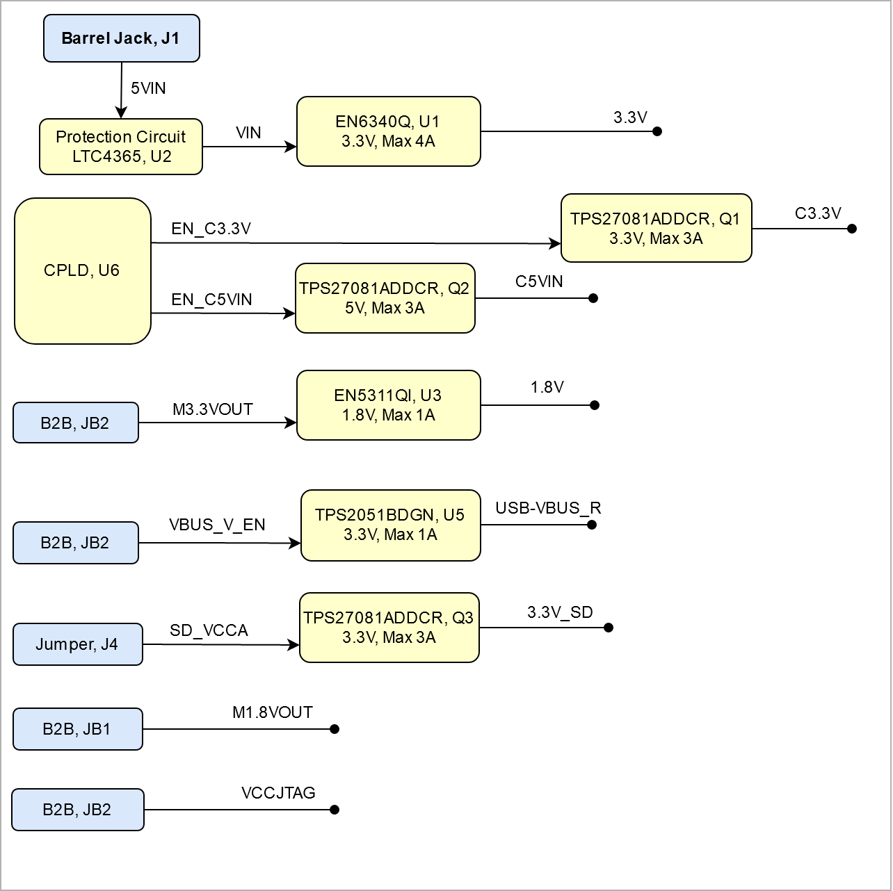 Image Removed Image Removed
|
Voltage Monitor Circuit
...
| anchor | Figure_PWR_VMC |
|---|
| title | Voltage Monitor Circuit |
|---|
| Scroll Ignore |
|---|
Create DrawIO object here: Attention if you copy from other page, objects are only linked. |
| Scroll Only |
|---|
image link to the generate DrawIO PNG file of this page. This is a workaround until scroll pdf export bug is fixed |
| Designator | Description | Frequency | Note |
|---|
|
| MHz |
|
|
| MHz |
|
|
| KHz |
|
|
|
|
|
|
Programmable Clock Generator
There is a programmable clock generator on-board (U??) provided in order to generate variable clocks for the module. Programming can be done using I2C via PIN header J??. The I2C Address is 0x??.
| Scroll Title |
|---|
| anchor | Table_OBP_PCLK |
|---|
| title | Programmable Clock Generator Inputs and Outputs |
|---|
|
| Scroll Table Layout |
|---|
| orientation | portrait |
|---|
| sortDirection | ASC |
|---|
| repeatTableHeaders | default |
|---|
| sortByColumn | 1 |
|---|
| sortEnabled | false |
|---|
| cellHighlighting | true |
|---|
|
U?? Pin
| Signal | Connected to | Direction | Note |
|---|
IN0 |
|
|
|
| | IN1 |
|
|
|
| | IN2 |
|
|
|
| | IN3 |
|
|
|
| XAXB |
|
|
|
| | SCLK |
|
|
|
| | SDA |
|
|
|
| | OUT0 |
|
|
|
| | OUT1 |
|
|
|
| | OUT2 |
|
|
|
| | OUT3 |
|
|
|
| | OUT4 |
|
|
|
| | OUT5 |
|
|
|
| | OUT6 |
|
|
|
| | OUT7 |
|
|
|
| | OUT8/OUT9 |
|
|
|
|
|
Power and Power-On Sequence
| Page properties |
|---|
|
In 'Power and Power-on Sequence' section there are three important digrams which must be drawn: - Power on-sequence
- Power distribution
- Voltage monitoring circuit
|
Power Supply
Power supply with minimum current capability of xx A for system startup is recommended.
Power Consumption
...
| Scroll Title |
|---|
| anchor | Table_PWR_PRPC |
|---|
| title | Module power rails.Power Consumption |
|---|
|
| Scroll Table Layout |
|---|
| orientation | portrait |
|---|
| sortDirection | ASC |
|---|
| repeatTableHeaders | default |
|---|
| style | |
|---|
| widths | |
|---|
| sortByColumn | 1 |
|---|
| sortEnabled | false |
|---|
| cellHighlighting | true |
|---|
|
Rail NameB2B Connector JM1 Pin | B2B Connector JM2 Pin | B2B Connector JM3 Pin | Direction | Notes | |
Bank Voltages
| Input Pin | Typical Current |
|---|
| VIN | TBD* |
|
* TBD - To Be Determined
Power Distribution Dependencies
| Scroll Title |
|---|
| anchor | TableFigure_PWR_BVPD |
|---|
| title | Zynq SoC bank voltages.Power Distribution |
|---|
|
tablelayout |
| orientation | portrait |
|---|
| sortDirection | ASC |
|---|
| repeatTableHeaders | default |
|---|
style | widths | | sortByColumn | 1 |
|---|
| sortEnabled | false |
|---|
| cellHighlighting | true |
|---|
| Schematic Name | | Notes |
|---|
...
...
use "include page" macro and link to the general B2B connector page of the module series,
...
? x ? modules use two or three Samtec Micro Tiger Eye Connector on the bottom side.
3 x REF-??????? (compatible to ????????), (?? pins, ?? per row)
| ignore |
|---|
| draw.io Diagram |
|---|
| border | false |
|---|
| |
|---|
| diagramName | TEB0707_PWR_PD |
|---|
| simpleViewer | false |
|---|
| width | 639 |
|---|
| links | auto |
|---|
| tbstyle | hidden |
|---|
| diagramDisplayName | |
|---|
| lbox | true |
|---|
| diagramWidth | 641 |
|---|
| revision | 2 |
|---|
|
|
| Scroll Only |
|---|
Image Added |
|
Power-On Sequence
| Scroll Title |
|---|
| anchor | Figure_PWR_PS |
|---|
| title | Power Sequency |
|---|
|
| Scroll Ignore |
|---|
| draw.io Diagram |
|---|
| border | false |
|---|
| |
|---|
| diagramName | TEB0707_PWR_PS |
|---|
| simpleViewer | false |
|---|
| width | 639 |
|---|
| links | auto |
|---|
| tbstyle | hidden |
|---|
| diagramDisplayName | |
|---|
| lbox | true |
|---|
| diagramWidth | 641 |
|---|
| revision | 1 |
|---|
|
|
| Scroll Only |
|---|
Image Added |
|
Voltage Monitor Circuit
| Scroll Title |
|---|
| anchor | Figure_PWR_VMC |
|---|
| title | Voltage Monitor Circuit |
|---|
|
| Scroll Ignore |
|---|
Create DrawIO object here: Attention if you copy from other page, objects are only linked. |
| Scroll Only |
|---|
image link to the generate DrawIO PNG file of this page. This is a workaround until scroll pdf export bug is fixed |
|
Power Rails
| Scroll Title |
|---|
| anchor | Table_PWR_PR |
|---|
| title | Module power rails. |
|---|
|
| Scroll Table Layout |
|---|
| orientation | portrait |
|---|
| sortDirection | ASC |
|---|
| repeatTableHeaders | default |
|---|
| style | |
|---|
| widths | |
|---|
| sortByColumn | 1 |
|---|
| sortEnabled | false |
|---|
| cellHighlighting | true |
|---|
|
| Power Rail Name | B2B Connector JM1 Pin | B2B Connector JM2 Pin | B2B Connector JM3 Pin | Direction | Notes |
|---|
|
|
|
|
|
|
|
|
|
|
|
|
|
|
|
|
|
|
|
|
|
|
|
|
|
Bank Voltages
| Scroll Title |
|---|
| anchor | Table_PWR_BV |
|---|
| title | Zynq SoC bank voltages. |
|---|
|
| Scroll Table Layout |
|---|
| orientation | portrait |
|---|
| sortDirection | ASC |
|---|
| repeatTableHeaders | default |
|---|
| style | |
|---|
| widths | |
|---|
| sortByColumn | 1 |
|---|
| sortEnabled | false |
|---|
| cellHighlighting | true |
|---|
|
|
Board to Board Connectors
| Page properties |
|---|
|
- This section is optional and only for modules.
use "include page" macro and link to the general B2B connector page of the module series, For example: 6 x 6 SoM LSHM B2B Connectors
| Include Page |
|---|
| PD:6 x 6 SoM LSHM B2B Connectors |
|---|
| PD:6 x 6 SoM LSHM B2B Connectors |
|---|
|
|
| Include Page |
|---|
| PD:4 x 5 SoM LSHM B2B Connectors |
|---|
| PD:4 x 5 SoM LSHM B2B Connectors |
|---|
|
...
Technical Specifications
Absolute Maximum Ratings
| Scroll Title |
|---|
| anchor | Table_TS_AMR |
|---|
| title | PS absolute maximum ratings |
|---|
|
| Scroll Table Layout |
|---|
| orientation | portrait |
|---|
| sortDirection | ASC |
|---|
| repeatTableHeaders | default |
|---|
| style | |
|---|
| widths | |
|---|
| sortByColumn | 1 |
|---|
| sortEnabled | false |
|---|
| cellHighlighting | true |
|---|
|
| Symbols | Description | Min | Max | Unit |
|---|
VV | V | V | V | V | V |
|
Recommended Operating Conditions
...
| Scroll Title |
|---|
| anchor | Table_TS_ROC |
|---|
| title | Recommended operating conditions. |
|---|
|
| Scroll Table Layout |
|---|
| orientation | portrait |
|---|
| sortDirection | ASC |
|---|
| repeatTableHeaders | default |
|---|
| style | |
|---|
| widths | |
|---|
| sortByColumn | 1 |
|---|
| sortEnabled | false |
|---|
| cellHighlighting | true |
|---|
| false |
|---|
| cellHighlighting | true |
|---|
|
| Parameter | Min | Max | Units | Reference Document |
|---|
|
|
| V | See ???? datasheets | | Parameter | Min | Max | Units | Reference Document |
|---|
| V | See ???? datasheets. | V | See Xilinx ???? datasheet. | V | See Xilinx ???? datasheet. | V | See Xilinx ???? datasheet. | V | See Xilinx ???? datasheet. | V | See Xilinx ???? datasheet. | V | See Xilinx ???? datasheet. | °C | See Xilinx ???? datasheet. |
|
|
| °C | See Xilinx ???? datasheet. |
|
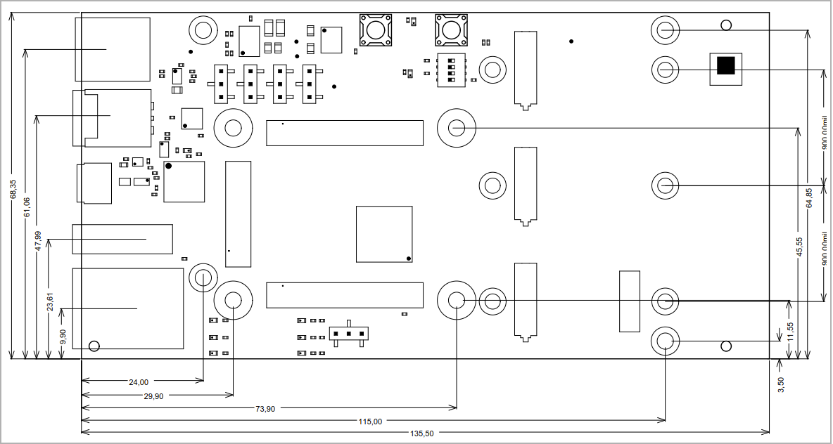
Physical Dimensions
Module size: ?? 135 mm × ?? 68 mm. Please download the assembly diagram for exact numbers.
Mating height with standard connectors: ? 4 mm.
PCB thickness: ?? 1.7 mm.
| Page properties |
|---|
|
In 'Physical Dimension' section, top and bottom view of module must be inserted, information regarding physical dimensions can be obtained through webpage for product in Shop.Trenz, (Download> Documents> Assembly part) for every SoM. For Example: for Module TE0728, Physical Dimension information can be captured by snipping tools from the link below: https://www.trenz-electronic.de/fileadmin/docs/Trenz_Electronic/Modules_and_Module_Carriers/5.2x7.6/TE0745/REV02/Documents/AD-TE0745-02-30-1I.PDF
|
...
| Scroll Title |
|---|
| anchor | Figure_TS_PD |
|---|
| title | Physical Dimension |
|---|
|
| Scroll Ignore |
|---|
| draw.io Diagram |
|---|
| border | false |
|---|
| |
|---|
| diagramName | TEB0707_TS_PD |
|---|
| simpleViewer | false |
|---|
| width | 639 |
|---|
| links | auto |
|---|
| tbstyle | hidden |
|---|
| diagramDisplayName | |
|---|
| lbox | true |
|---|
| diagramWidth | 641 |
|---|
| revision | 16 |
|---|
|
|
| Scroll Only |
|---|
| scroll-pdf | true |
|---|
| scroll-office | true |
|---|
| scroll-chm | true |
|---|
| scroll-docbook | true |
|---|
| scroll-eclipsehelp | true |
|---|
| scroll-epub | true |
|---|
| scroll-html | true |
|---|
| 
|
|
...
| Scroll Title |
|---|
| anchor | Table_RH_HRH |
|---|
| title | Hardware Revision History |
|---|
|
| Scroll Table Layout |
|---|
| orientation | portrait |
|---|
| sortDirection | ASC |
|---|
| repeatTableHeaders | default |
|---|
| style | |
|---|
| widths | |
|---|
| sortByColumn | 1 |
|---|
| sortEnabled | false |
|---|
| cellHighlighting | true |
|---|
|
| Date | Revision | Changes | Documentation Link |
|---|
| 2020-04-01 | REV01 | Initial Release |
|
|
Hardware revision number can be found on the PCB board together with the module model number separated by the dash.
...