Page History
| Custom_table_size_100 |
|---|
| Page properties | ||||
|---|---|---|---|---|
| ||||
Template Revision 2.9 - on construction Design Name always "TE Series Name" + optional CPLD Name + "CPLD"
|
Overview
A Lattice XO2-1200 CPLD (U19) is used as a System Management Controller. The SC is responsible for power sequencing, reset generation and zynq initial configuration (mode pin strapping). Moreover, some on-board ICs are connected to the SC that provides level shifting. The SC wakes up when the 3.3V input power rises above 2.1V (VIN voltage is not needed). The SC can turn on or off all of the other supplies on the module (except in no power sequencing mode when the 1.0V and 1.8 V supplies are forced to start immediately when power is applied to the module).
System Controller (SC) was designed to allow ZYNQ PS system to access module special functions as early as possible without reducing the number of MIO pins that are fully user configurable.This early communication channel is done using MIO52 and MIO53 pins that are used also as ethernet PHY management interface for the on-board gigabit PHY. In order to simplify the boot process and reduce the number of time the PS peripherals need to be configured or re-initialized SC uses the same protocol on MIO52/MIO53 as the Gigabit PHY itself. This means that FSBL configures all peripherals to their final function, allocating MIO52 and MIO53 as ethernet MDIO interface. SC controller appears as "Virtual Ethernet PHY" on the MDIO bus of PS ethernet 0 interface. This interface is already available when Zynq PL Fabric is not configured. It would have been possible to use I2C protocol on MIO52/MIO53 but in such case some multiplexing would be needed to choose between two protocols, also it would be needed to change the peripheral mapping after first init by the FSBL. For use cases where ethernet PHY on TE0720 is not used at all, it is still possible to configure SC with design that implements I2C protocol on MIO52/MIO53 pins.For most use cases the only need to use this interface is access to MAC address info, this is normally done by u-boot loader that fetches the MAC address bytes and sets its environment variables accordingly. Linux image will then also be started so that the MAC address from EEPROM is used for ethernet 0 physical interface.
Feature Summary
Power Management
- Reset Management
JTAG Routing
Boot Mode
User IO
LED
- MDIO Interface
- UNI/O MAC access
- Watchdog Timer
- I2C
Firmware Revision and supported PCB Revision
See Document Change History
Product Specification
Port Description
Name / opt. VHD Name | Direction | Pin | Pullup/Down | Bank Power | Description |
|---|---|---|---|---|---|
BOOT_R / BOOTMODE_R | out | N12 | NONE | 3.3V | If low then the QSPI flash can not be written. (Write protect) |
BOOT_R5 / BOOTMODE_R5 | out | M11 | DOWN | 3.3V | If low then the QSPI flash will be reset. (HOLD/RESET) |
CLK_125MHz | in | G13 | NONE | 1.8V | 125MHZ Clock Output of Ethernet transceiver chip (88E1512-A0-NNP2C000) that synchronized with the 25MHZ reference clock |
EN_3V3 | out | A2 | DOWN | 3.3V | If high then the 3.3V power will be switched ON. |
EN1 | in | A9 | UP | 3.3V | User Enable. Enables the DC-DC converters and on board supplies (Active High). (B2B JM1-28)(DIP Switch on the carrier board) . Not used if NOSEQ = '1' |
ETH-CLK-EN / EN_ETH_CLK | out | J14 | NONE | 1.8V | ETH clock enable. Enable pin for U9 oscillator chip U9 (SiT8008BI-73-18S-25.000000E) to feed a clock to Ethernet Transceiver(U8). Default is mapped to logic high '1'. Enabled as default. |
ETH-MDC / mdc | in | L14 | UP | 1.8V | Management Data Clock reference for the Ethernet transceiver chip. This pin is connected with MIO52 of FPGA too and can be activated in Zynq7 adjustment. |
ETH-MDIO / mdio | inout | K14 | UP | 1.8V | It is Management Data pin of Ethernet transceiver chip to transfer in and out of the device synchronously to mdc. It is connected with MIO53 of FPGA. |
ETH-RST | out | E14 | DOWN | 1.8V | ETH PHY RESET. Reset pin of Ethernet transceiver chip. (Active low) Default is mapped to internal reset. |
INIT | in | C9 | UP | 3.3V | INIT_B_0 pin of FPGA. (Active low). This pin must be tristate for PL configuratuion. By user or device held low until is ready to be configured. |
INT1 / INT2 | in | P4 | UP | 3.3V | MEMS Interrupt 1 of 3D accelerometer and 3D magnetometer chip U22 (LSM303DTR) (Active High) |
INT2 / INT1 | in | P6 | UP | 3.3V | MEMS Interrupt 2 of 3D accelerometer and 3D magnetometer chip U22 (LSM303DTR) (Active High) |
JTAGMODE | in | B9 | 3.3V | JTAGENB pin of CPLD. Enable JTAG access to CPLD for Firmware update (zero: JTAG routed to module, one: CPLD access) | |
LED1 | out | P2 | NONE | 3.3V | Display green LED (D2). Default mapped to MIO7 |
LED2 | out | N3 | DOWN | 3.3V | Display red LED (D5). Default mapped to modeblink. In this case LED flashs depending on the boot mode (SD card → slow, QSPI → fast) |
MEM-MAC / MAC_IO | inout | M14 | UP | 1.8V | Serial Clock/Data input/Output of Serial EEPROM (11AA02E48T-I/TT) U17 |
MEM-SHA / SHA_IO | inout | N14 | UP | 1.8V | SDA for CryptoAuthentication Chip (ATSHA204A-STUCZ-T) U10 |
MIO14 | inout | M4 | NONE | 3.3V | This pin is connected to Zynq PS-MIO (B6) . (RX pin of UART0) |
MIO15 | inout | N4 | NONE | 3.3V | This pin is connected to Zynq PS-MIO (E6) . (TX pin of UART0) |
MIO7 | in | P11 | UP | 3.3V | This pin is used as GPIO. |
MMC_RST | out | G14 | DOWN | 1.8V | eMMC reset. Reset pin of eMMC memory (MTFC16GJVEC-2M WT) U15. Default is mapped to internal reset. |
MODE / BOOTMODE_IN | in | C8 | UP | 3.3V | Latched as BOOTMODE once at power-up, can be used later as I/O, weak pull up. Force low for boot from the SD Card. Latched at power on only, not on soft reset (B2B-JM1 pin 32) |
MODE / BOOTMODE_IN2 | in | M9 | UP | 3.3V | Latched as BOOTMODE once at power-up, can be used later as I/O, weak pull up. Force low for boot from the SD Card. Latched at power on only, not on soft reset (B2B-JM1 pin 32) |
MR / POR_B | out | P12 | UP | 3.3V | Power-on-reset pin. This pin is connected with supply voltage monitor chip (TPS3106K33DBVR) U26 and controls the PS_POR_B pin of FPGA. (Active Low) |
NetU19_B12 | B12 | / currently_not_used | |||
NetU19_B13 | B13 | / currently_not_used | |||
NetU19_B2 | B2 | / currently_not_used | |||
NetU19_B3 | B3 | / currently_not_used | |||
NetU19_B7 | B7 | / currently_not_used | |||
NetU19_C1 | C1 | / currently_not_used | |||
NetU19_C10 | C10 | / currently_not_used | |||
NetU19_C12 / Dummy | out | C12 | DOWN | 3.3V | |
NetU19_C3 | C3 | / currently_not_used | |||
NetU19_C6 / RST | in | C6 | UP | 3.3V | |
NetU19_C7 | C7 | / currently_not_used | |||
NetU19_E1 | E1 | / currently_not_used | |||
NetU19_E12 | E12 | / currently_not_used | |||
NetU19_F13 | F13 | / currently_not_used | |||
NetU19_F3 | F3 | / currently_not_used | |||
NetU19_G3 | G3 | / currently_not_used | |||
NetU19_H3 | H3 | / currently_not_used | |||
NetU19_J3 | J3 | / currently_not_used | |||
NetU19_K13 | K13 | / currently_not_used | |||
NetU19_K3 | K3 | / currently_not_used | |||
NetU19_L3 | L3 | / currently_not_used | |||
NetU19_M12 | M12 | / currently_not_used | |||
NetU19_M2 | M2 | / currently_not_used | |||
NetU19_M3 | M3 | / currently_not_used | |||
NetU19_N13 | N13 | / currently_not_used | |||
NetU19_N5 | N5 | / currently_not_used | |||
NetU19_N7 | N7 | / currently_not_used | |||
NetU19_N8 | N8 | / currently_not_used | |||
NOSEQ | inout | A3 | DOWN | 3.3V | Usage CPLD Variant depends. (B2B-NOSEQ pin 7) Forces the 1.0V and 1.8V DC-DC converters always ON when high. Can be used as an I/O after boot. Default mapped to PHY_LED0. |
ON_1V0 | out | A12 | NONE | 3.3V | Enable pin for 1.0 V DC-DC (Active High) |
ON_1V5 | out | M7 | NONE | 3.3V | Enable pin for 1.5 V DC-DC (Active High) |
ON_1V8 | out | A11 | NONE | 3.3V | Enable pin for 1.8 V DC-DC (Active High) |
OTG-RST | out | B14 | DOWN | 1.8V | USB PHY reset. Reset pin for high speed USB transceiver (USB3320C-EZK) U18 (Active Low). Default is mapped to internal reset. |
PG_1V0 | in | A7 | UP | 3.3V | Power OK (POK) pin of 1.0V DC-DC converter EN6347QI (U1). If High then the output voltage of regulator is within 10% of nominal value (OK). |
PG_1V5 | in | N6 | UP | 3.3V | Power OK (POK) pin of 1.5V DC-DC converter EP53F8QI (U2). If High then the output voltage of regulator is Ok. |
PG_1V8 | in | A10 | UP | 3.3V | Power OK (POK) pin of 1.8V DC-DC converter EP53F8QI (U3). If High then the output voltage of regulator is Ok. |
PG_3V3 / POR | in | C11 | UP | 3.3V | POR Reset pin. This pin is connected with PG_3V3. As long as the VCCIO34 voltage is zero, this pin will remain low. |
PGOOD | inout | B8 | UP | 3.3V | Power good output as default, can be used as I/O. (B2B JM1-Pin 30) Forced low until all on-board power supplies are working properly. |
PHY_CONFIG | inout | C14 | DOWN | 1.8V | ETH PHY CONFIG. Hardware configuration pin of Ethernet transceiver (88E1512-A0-NNP2C000). Default mapped to logic low '0'. Therefore PHY address set to 0x00. |
PHY_LED0 | inout | F14 | NONE | 1.8V | LED output 0 of Ehternet transceiver chip |
PHY_LED1 | inout | D12 | NONE | 1.8V | LED output 1 of Ehternet transceiver chip |
PHY_LED2 | inout | C13 | NONE | 1.8V | LED output 2 or interrupt output pin (Active Low) of Ehternet transceiver chip |
PJTAG_R | out | N10 | NONE | 3.3V | This pin in the schematic is connected with SPI-DQ0/M0 Pin |
PROG_B | in | A13 | UP | 3.3V | By pulsing this pin any configuration that is currently loaded is cleared and the PL prepared to load new configuration. (Active Low) Default is mapped to logic high '1'. |
PS-RST / SRST_B | out | M13 | UP | 1.8V | PS software reset (Active Low). Default is mapped to logic high '1'. |
PUDC_B | inout | E3 | DOWN | VCCIO34 | Selects the enable or disable of pull-ups during configuration on the user I/O pins. (Active Low) Enables internal pull-up resistors on the select I/O pins after power-up and during configuration. Default is mapped to logic low '0'. |
RESIN | in | C4 | UP | 3.3V | Master reset input (Active Low). Default mapping forces POR_B reset to Zynq PS |
RST / RST_SENSE | in | P3 | NONE | 3.3V | Reset pin that is connected with PS_PORT_B (Power-on-reset) (Active Low) |
RTC_INT | in | N2 | UP | 3.3V | Interrupt output or frequency output of RTC chip (ISL12020MIRZ) U20 (Active Low) |
SCL | inout | P8 | UP | 3.3V | I2C clock pin of MEMS chip (LSM303DTR) U22 |
SDA | inout | P7 | UP | 3.3V | I2C data pin of MEMS chip (LSM303DTR) U22 |
SPK_L | M5 | / currently_not_used | |||
SPK_R | M8 | / currently_not_used | |||
TCK / C_TCK | out | P13 | DOWN | 3.3V | Zynq JTAG clock pin |
TDI / C_TDI | out | P9 | DOWN | 3.3V | Zynq JTAG data input pin |
TDO / C_TDO | in | M10 | DOWN | 3.3V | Zynq JTAG data output pin |
TMS / C_TMS | out | N9 | DOWN | 3.3V | Zynq JTAG mode select pin |
VCCIO34 | E2 | / currently_not_used | |||
VCCIO34 | F2 | / currently_not_used | |||
VCCIO34 | H2 | / currently_not_used | |||
VCCIO34 | J2 | / currently_not_used | |||
VCCIO34 | K2 | / currently_not_used | |||
X_TCK / M_TCK | in | B6 | DOWN | 3.3V | FTDI JTAG clock pin (B2B-JM1-pin 99) |
X_TDI / M_TDI | in | B4 | DOWN | 3.3V | FTDI JTAG data input pin (B2B-JM1-pin 95) |
X_TDO / M_TDO | out | A4 | DOWN | 3.3V | FTDI JTAG data output pin (B2B-JM1-pin 97) |
X_TMS / M_TMS | in | A6 | DOWN | 3.3V | FTDI JTAG mode select pin (B2B-JM1-pin 93) |
X1 | in | F1 | UP | VCCIO34 | CPLD pin to the FPGA (L16). I2C clock from FPGA |
X2 / XIO4 | inout | C2 | UP | VCCIO34 | CPLD pin to the FPGA (M15). Default mapped to PHY_LED0 (ETH PHY LED0). |
X3 / XIO5 | inout | B1 | UP | VCCIO34 | CPLD pin to the FPGA (N15). Default mapped to PHY_LED1 (ETH PHY LED1). |
X4 / XIO6 | inout | D1 | UP | VCCIO34 | CPLD pin to the FPGA (P16). Default mapped to PHY_LED2 (ETH PHY LED2). |
X5 | out | J1 | NONE | VCCIO34 | CPLD pin to the FPGA (P22). I2C data to FPGA |
X6 | H1 | / currently_not_used | |||
X7 | in | M1 | UP | VCCIO34 | CPLD pin to the FPGA (N22). I2C data from FPGA |
XCLK | out | K1 | NONE | VCCIO34 | CPLD pin to the FPGA (K19). Default mapped to CLK_125MHZ. (Clock output of ethernet transceiver chip) |
- / SIG1 | in | E13 | NONE | 1.8V | This pin is connected with VCCIO34 directly in the schematic REV03 and has no lable in the schematic. |
Functional Description
To access and control the following functions it must be accessed CR registers. For more information about how to access these registers refer to 111447303
JTAG
JTAG signals routed directly through the CPLD to FPGA. Access between CPLD and FPGA can be multiplexed via JTAGENB pin of CPLD (B9) (logical one for CPLD, logical zero for FPGA). This pin is connected to B2B (JM1-pin 89) directly. On the carrier board can be this pin enabled or disabled with a dip switch.
CPLD JTAGENB (B2B JM1-89) | Description |
|---|---|
0 | FPGA access |
1 | CPLD access |
Boot Mode
TE0720 supports QSPI and SD card boot modes. Boot mode depends on the logic state of MODE pin of CPLD. This pin is directly connected to B2B connector.
| CPLD MODE Pin (B2B Pin JM1-32) | BOOT MODE |
|---|---|
| 0 | SD Card |
| 1 | QSPI |
Watchdog Timer
Watchdog timer is an added option in the CPLD code. To control and to use watchdog timer correctly , it must be written correct values in the related CR registers.
Watchdog timer signal / register | Related CPLD Register | Access in FSBL code | Access in Linux | Description |
|---|---|---|---|---|
WDT input clock | CR1(14) CR1 = Register5 | XEmacPs_PhyWrite / XEmacPs_Phyread | Phytool command | |
WDT_time | CR4[7:0] CR4 = Register12 | XEmacPs_PhyWrite / XEmacPs_Phyread | Phytool command | If CR4[7:0] = 0x00 → WDT_time = 0x07 |
WDT_Enable | CR3[15:8] CR3 = Register7 | XEmacPs_PhyWrite / XEmacPs_Phyread | Phytool command | If CR3[15:8] = 0xA5 → WDT enable If CR3[15:8] /= 0xA5 → WDT disable |
For example to access these registers in FSBL code it can be used the following instruction:
Status = XEmacPs_PhyWrite(&Emac, 0x1A, 7, 0xA500); if(Status != XST_SUCCESS){ return XST_FAILURE; } → To enable WDTStatus = XEmacPs_PhyWrite(&Emac, 0x1A, 7, 0x0000); if(Status != XST_SUCCESS){ return XST_FAILURE; } → To disable WDTStatus = XEmacPs_PhyWrite(&Emac, 0x1A, 12, 0x001F); if(Status != XST_SUCCESS){ return XST_FAILURE; } → To adjust desired time for WDT
Another way to access the related registers for WDT is to use phytool command. It must be added the ethtool package in Linux. To add this package it must be chosen in petalinux configuration for rootfs this option. The path in petalinux rootfs is: Filesystem packages/console/network/ethtool
The phytool instruntion format is :
Phytool read device/addr/register
Phytool write device/addr/register <value>
To write desired value in the related WDT registers for example can be written the following instructions in Linux console:
phytool write eth0/0x1A/7 0xA500 → WDT enable
phytool write eth0/0x1A/7 0x0000 → WDT disable
phytool write eth0/0x1A/12 0x001F → Adjusted WDT time. It depends on the period of the CPLD clock.
phytool write eth0/0x1A/5 0x4000 → To set the WDT input clock high
phytool write eth0/0x1A/5 0x0000 → To set the WDT input clock low
If the WDT is activated and the generated clock is fed to WDT input clock , it will not be reset the board (WDT_RST signal low). But if the generation of this clock is stopped , the board will be reset (WDT_RST signal high) after a period of time depending on the WDT_time (CR4[7:0] register value).
To test Watchdog timer can be fed a clock signal to WDT clock input. The following shell script file generates a clock for WDT input clock. This file must be copied as init.sh to the SD card additionally. This shell script file will be executed by booting the board and generates the WDT input clock automatically. As long as 1 key and enter key is not pressed, the WDT clock will be generated and subdequently the board will not be reset. But if genetation of clock signal be stopped, the boad will be reset after a period of time. Note that WDT must already be activated in FSBL code.
| Code Block | ||||
|---|---|---|---|---|
| ||||
#WDT test
#!/bin/sh
echo "Starting the WDT Clock"
sleep 1
while :
do
    phytool read eth0/0x1A/5
    phytool write eth0/0x1A/5 0x4041
    sleep 0.5
    phytool read eth0/0x1A/5
    phytool write eth0/0x1A/5 0x0041
    sleep 0.5
	read -r -t 0.1 b
	echo "Press 1 to exit!"
    if (( b == 1 )) ; then
      break
    fi
done
printf "\Quit.......................\n\n" |
Reset
Zynq will be reset, when it occures one of the following conditions:
Reset name | Reset reasone | related reset pin / signal | Active |
|---|---|---|---|
Reset | Reset push button | RESIN | LOW |
Reset command in software | CR1(15) | HIGH | |
WDT reset | Overflowing the WDT counter and no existance WDT input clock (For more information refer to 111447303) | WD_RST | HIGH |
Extra Reset
The board can also be reset through software.
Extra reset | related register | Access in FSBL code | Access in Linux | Description |
|---|---|---|---|---|
Enable register | CR3[15:8] CR3 = Register7 | XEmacPs_PhyWrite / XEmacPs_Phyread | Phytool command | If CR3[15:8] = 0xE5 → Extra reset enable If CR3[15:8] /= 0xE5 → Extra reset disable |
Reset bit | CR1(15) | --- | Phytool command | If CR1(15) = '1' → Reset the board |
For example the following instructions can reset the board:
phytool write eth0/0x1A/7 0xE500 → Extra reset enable
phytool write eth0/0x1A/5 0x8000 → Reset the board
It can be activated this option in FSBL code too:
Status = XEmacPs_PhyWrite(&Emac, 0x1A, 7, 0xE500); if(Status != XST_SUCCESS){ return XST_FAILURE; }
Serial EEPROM
The seial EEPROM (U17) is used to save MAC addess. The MAC_IO pin of EEPROM uses UNI/O interface to communicate with CPLD. The connection between EEPROM chip and CPLD depends on the value of XIO4.
XIO4[3:0] | MAC_IO |
|---|---|
0011 | '0' |
else | Connected to internal MAC read block |
CryptoAuthentication
The CryptoAuthentication chip (U10) is a high-security hardware authentication device that allows use in many application same as checking user password. This device can communicate with 1MHZ I2C interface,single-wire interface or UART.
XIO4[3:0] | Value XIO5 | SHA_IO |
|---|---|---|
0010 | '0' | '0' |
else | 'Z' | |
UART
CR2[7:4] | MIO14 (RX) | Description |
|---|---|---|
1001 | XIO5_in | XIO5_in is equal to XIO5 if VCCIO34 voltage equal to 1.8V. |
else | 'Z' | |
CR2[11:8] | MIO15 (TX) | Description |
1001 | XIO6_in | XIO6_in is equal to XIO6 if VCCIO34 voltage equal to 1.8V. |
else | 'Z' |
I2C to GPIO block
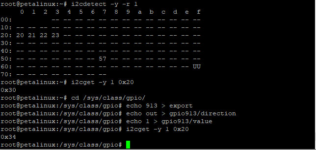
This subsystem provides 32-bit (4 x 8-bit) of general purpose parallel input and output (I/O) expansion for the I2C bus protocol. This module contain of four 8-bit registers that the GPIO data can be saved in this registers with addresses from 0x20 to 0x23. It can be accessed this register with I2C commands in linux console or with i2c functions in FSBl code. To access the registers of the subsystem can be used the following commands in linux console:
To see the i2c bus addresses : i2cdetect -y -r 1
To read first register with address 0x20 : i2cget -y 1 0x20
To write for example 0x55 in first register with address 0x20 : i2cset -y 1 0x20 0x55
| Scroll Title | ||||||||||||||||||||||
|---|---|---|---|---|---|---|---|---|---|---|---|---|---|---|---|---|---|---|---|---|---|---|
| ||||||||||||||||||||||
|
The MIO7 pin is connected to third bit of GPIO input of the I2C to GPIO subsystem (register address 0x20).To test the I2C to GPIO subsystem the MIO7 state can be changed and the value of the first register (register address 0x20) can be monitored. The initial value of this register depends on the CPLD firmware and can be variable. In the following example the initial value of this register is equal to 0x30. That means that initial value of MIO7 is zero. Now set MIO7 to one and read the value of the first register with address 0x20 again. It should be equal to 0x34.
To read the first register of the subsystem:
i2cget -y 1 0x20 → For example here is equal to 0x30.
To set MIO7 to one:
cd /sys/class/gpio/
echo 913 > export
echo out > gpio913/direction
echo 1 > gpio913/value
To read the first register of the subsystem again:
i2cget -y 1 0x20 → It should be equal to 0x34.
| Scroll Title | ||
|---|---|---|
| ||
|
The subsystem I2C to GPIO port mapping is according the following table:
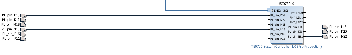
I2C to GPIO | Pin name | CPLD Pin | Direction | FPGA Pin | Description |
|---|---|---|---|---|---|
sda_in | X7 | M1 | from FPGA | N22 | |
sda_out | X5 | J1 | to FPGA | P22 | If X7 is Low, this pin will be disconnected. |
sclk | X1 | F1 | from FPGA | L16 | |
| SDA | SDA | P7 | To/From RTC and MEMS | -- | I2C data pin of ISL12020MRZ RTC chip / I2C data pin of MEMS chip (LSM303DTR) U22 |
| SCL | SCL | P8 | To RTC and MEMS | -- | I2C clock pin of ISL12020MRZ RTC chip / I2C clock pin of MEMS chip (LSM303DTR) U22 |
GPIO_input | Mapping the GPIO_input bits to various ports or signals | ||||
GPIO_output | Not used | ||||
GPIO input bit mapping:
GPIO_input bit | Connected to: |
|---|---|
0 | PHY_LED0 |
1 | PHY_LED1 |
2 | MIO7 |
3 | NOSEQ |
4 | RESIN_g |
5 | EN1_g |
6 | BOOTMODE_LATCHED |
7 | BOOTMODE_IN |
8 | INT1 |
9 | INT2 |
10 | RTC_INT |
11 | PHY_LED2 |
12 | '0' |
13 | '0' |
UNI/O MAC read block
UNI/O bus is a low speed serial interface for embedded systems that requires only one logic signal SCIO (Serial Clock, Data Input/Output). By using Manchester encoding techniques, the clock and data are combined into a single, serial bit stream (SCIO),where the clock signal is extracted by the receiver to correctly decode the timing and value of each bit. The serial EEPROM (U17) interface is UNI/O. The UNI/O bus uses a master/slave configuration. In this system the serial EEPROM chip is slave and a UNI/O subsystem in CPLD works as master. Both master and slave can operate as transmitter or receiver, but the master device determines which mode is active.The UNI/O MAC read block in CPLD reads the MAC address from serial EEPROM chip during power-on.
| Scroll Title | ||||||||||||||||||||||
|---|---|---|---|---|---|---|---|---|---|---|---|---|---|---|---|---|---|---|---|---|---|---|
| ||||||||||||||||||||||
|
uio_sm_cnt[8:5] | uio_io_data |
|---|---|
0000 | MIO7 |
0001 | RTC_INT |
0010 | INT1 |
0100 | INT2 |
0011 | PHY_LED0 |
0100 | PHY_LED1 |
0101 | PHY_LED2 |
0110 | BOOTMODE_IN |
0111 | MIO14 |
1000 | MIO15 |
1001 | XIO4 |
1010 | XIO5 |
1011 | XIO6 |
1100 | WD_HIT |
1101 | '0' |
1110 | '0' |
Multiplexing uio data output between uio-id and uio-io:
uio_sm_cnt[2:1] | uio_sm_cnt(4) | uio_unidir |
|---|---|---|
01 | - | '0' |
10 | '0' | uio_id_data |
10 | '1' | uio_io_data |
SC Pins to B2B
Name | B2B | Mode | Default function | Alternative | Description |
|---|---|---|---|---|---|
EN1 | JM1-Pin 28 | input, weak pull-up | Power Enable | IO | High enables the DC-DC converters and on-board supplies. Not used if NOSEQ=1 |
MODE | JM1-Pin 32 | input, weak pull-up | Boot mode | SDA or IO | Force low for boot from the SD Card. Latched at power on only, not on soft reset! |
NOSEQ | JM1-Pin 7 | input, weak pull-down | Power sequencing Control | Output | Forces the 1.0V and 1.8V DC-DC converters always ON when high. Can be used as an I/O after boot. |
PGOOD | JM1-Pin 30 | output, open drain | Power good | SCL or IO | Forced low until all on-board power supplies are working properly. Attention: During CPLD programming, this pins is high impedance. |
RESIN | JM2-Pin 18 | input, weak pull-up | Reset input | IO | Active Low Reset input, default mapping forces POR_B reset to Zynq PS |
SC Pins to FPGA
Schematic net name | VHDL Name | Default function | Direction | SC pin | FPGA pin | Description |
|---|---|---|---|---|---|---|
XCLK | XCLK | ETH PHY Clock to FPGA | to FPGA | K1 | K19 | |
X7 | X7 | I2C Data from FPGA | from FPGA | M1 | N22 | SDA from EMIO I2Cx |
X5 | X5 | I2C Data to FPGA | to FPGA | J1 | P22 | SDA to EMIO I2Cx |
X4 | XIO6 | ETH PHY LED2 (PHY_LED2) | to FPGA | D1 | P16 | |
X3 | XIO5 | ETH PHY LED1 (PHY_LED1) | to FPGA | B1 | N15 | RTC, MEMS Interrupt or PHY LED1 |
X2 | XIO4 | ETH PHY LED0 (PHY_LED0) | to FPGA | C2 | M15 | |
X1 | X1 | I2C Clock from FPGA | from FPGA | F1 | L16 | SCL from EMIO I2Cx |
PUDC_B | PUDC_B | Enables internal pull-up resistors on the IOs | to FPGA | E3 | K16 | normally not used tied to fixed level by SC |
NOSEQ Pin
This is a dedicated input that forces the module's 1.0V and 1.8V supplies to be enabled if high. This pin has a weak pull-down on the module. If left open the module will power up in normal power sequencing enabled mode. This pin is 3.3V tolerant. This pin is also connected to the System Management Controller. The SC can read the status of this pin (it can be detected if the module is in power sequencing enabled mode). The SC can also use this pin as output after normal power on sequence.
No Sequencing mode
If the module is powered from a single 3.3V supply and power sequencing is disabled, then NOSEQ pin should be powered from the main 3.3V input. That is VIN, 3.3Vin and NOSEQ should all be tied together to the input 3.3V power rail. Sequencing mode should not be used if VIN is not 3.3V.
Normal mode
For normal operation leave NOSEQ open or pull down with a resistor.
Normal mode with user function on NOSEQ
NOSEQ can be used as an output after boot. NOSEQ must be low when 3.3V power is applied to the module. Common usage is an LED connected between NOSEQ and GND. The mapping of NOSEQ pin can be changed by CR1 register. The CR1 register is control register of MDIO slave interface that its content can be changed with FSBL code, uboot command or in linux console directly.
SC MDIO Interface
Most registers and functions are available via ETH PHY Management interface (MIO pins 52 and 53).
Address
Addr | R/W | Register name | Descripion |
|---|---|---|---|
0 | RO | ||
1 | RO | ||
2 | RO | ID1 | PHY Identifier Register 1 |
3 | RO | ID2 | PHY Identifier Register 2 |
4 | RW | ID3 | PHY Identifier Register 3 |
5 | RW | CR1 | Control Register 1: LED's |
6 | RW | CR2 | Control Register 2; XIO Control |
7 | RW | CR3 | Control Register 3; Reset, Interrupt |
8 | RO | SR1 | Status Register |
9 | RO | MAChi | Highest bytes of primary MAC Address |
0xA | RO | MACmi | Middle bytes of primary MAC Address |
0xB | RO | MAClo | Lowest bytes of primary MAC Address |
0xC | RO | CR4 | reserved do not use |
0xD | RW | MMD_CR | MMD Control Register |
0xE | RW | MMD_AD | MMD Address/Data |
0xF | - | reserved do no use | |
other | - | reserved do not use |
Register Overview
Register CR1
CR1 | related function |
|---|---|
15 | Enable Extra_Enable |
14 | WD_HIT generation |
13 | Undefined |
12 | Undefined |
11:8 | NOSEQ Mux |
7:4 | LED1 Mux |
3:0 | LED2 Mux |
Register CR2
CR2 | related function |
|---|---|
15:12 | XCLK Mux |
11:8 | XIO6 Mux |
7:4 | XIO5 Mux |
3:0 | XIO4 Mux |
Register CR3
CR3 | related port/signal |
|---|---|
0 | INT1 |
1 | INT2 |
2 | RTC_INT |
3 | PHY_LED2 |
4 | OTG_RST |
5 | ETH_RST |
6 | MMC_RST |
7 | EN_ETH_CLK |
15:8 | WDT enable/ Extra enable |
Register CR4
CR4 | related function |
|---|---|
7:0 | WDT time |
| 15:8 | Undefined |
Register SR1
SR1 | related function |
|---|---|
0 | INT1 |
1 | INT2 |
2 | RTC_INT |
3 | PHY_LED2 |
7 | BOOTMODE_LATCHED |
8 | BOOTMODE_IN2 |
9 | BOOTMODE_IN |
10 | NOSEQ |
11 | NOSEQ_LATCHED |
12 | WD_EVENT |
13 | PG_1V5 |
14 | EXTRA_ENABLED or WDOG_ENABLED |
15 | mac_valid |
Register Details
Register CR1
The mapping of LED1(Green) , LED2(Red) and NOSEQ pin depends on the value of CR1 register.
CR1[3:0] | LED1 (Green) D2 | CPLD | Description |
|---|---|---|---|
0001 | PHY_LED0 | Input/Output | LED output 0 of Ehternet transceiver chip |
0010 | PHY_LED1 | Input/Output | LED output 1 of Ehternet transceiver chip |
0011 | PHY_LED2 | Input/Output | LED output 2 or interrupt output pin (Active Low) of Ehternet transceiver chip |
0100 | MIO7 | Input | GPIO |
0101 | RTC_INT | Input | Interrupt output or frequency output of RTC chip |
0110 | OFF | ||
0111 | ON | ||
1000 | XIO4 | Input/Output | CPLD pin to the FPGA (M15). ETH PHY LED0 |
1001 | Not MIO14 | Input/Output | |
1010 | Not MIO14/Not MIO15 | Input/Output | |
others | MIO7 | Input | Default value for CR1[3:0] is 0000. GPIO |
CR1[7:4] | LED2 (Red) D5 | CPLD | Description |
0001 | PHY_LED0 | Input/Output | LED output 0 of Ehternet transceiver chip |
0010 | PHY_LED1 | Input/Output | LED output 1 of Ehternet transceiver chip |
0011 | PHY_LED2 | Input/Output | LED output 2 or interrupt output pin (Active Low) of Ehternet transceiver chip |
0100 | MIO7 | Input | GPIO |
0101 | RTC_INT | Input | Interrupt output or frequency output of RTC chip |
0110 | OFF | ||
0111 | ON | ||
1000 | XIO5 | Input/Output | CPLD pin to the FPGA (N15). ETH PHY LED1 |
1001 | Not MIO15 | Input/Output | |
1010 | Not MIO14/Not MIO15 | Input/Output | |
others | modeblink | Signal | If SD card boot mode is selected on the carrier board (for examle for TE0703 S2-4 DIP switch ON) , LED2 flashs slow otherweise LED2 flashs fast. |
CR1[11:8] | NOSEQ | CPLD | Description |
0001 | PHY_LED0 | Input/Output | LED output 0 of Ehternet transceiver chip |
0010 | PHY_LED1 | Input/Output | LED output 1 of Ehternet transceiver chip |
0011 | PHY_LED2 | Input/Output | LED output 2 or interrupt output pin (Active Low) of Ehternet transceiver chip |
0100 | MIO7 | Input | GPIO |
0101 | RTC_INT | Input | Interrupt output or frequency output of RTC chip |
0110 | OFF | ||
0111 | ON | ||
1000 | XIO6 | Input/Output | CPLD pin to the FPGA (P16). ETH PHY LED2 |
1001 | uio_unidir | Signal | |
1010 | Undefined | ||
others | PHY_LED0 | Input/Output | Default value for CR1[11:8] is 0000. LED output 0 of Ehternet transceiver chip |
| CR1(12) | --- | --- | --- |
| --- | Undefined | --- | --- |
| CR1(13) | --- | --- | --- |
| --- | Undefined | --- | --- |
| CR1(14) | WDT Counter | CPLD | Description |
| 0 | counts | Register | CR1(14) = WD_HIT If WD_HIT = '0' --> If WD_counter = WD_time --> WD_RST = '1' --> WD happens |
| 1 | reset | Register | If WD_HIT = '1' --> WD_RST = '0' --> WD will not happen and the WD_counter will be reset. |
| CR1(15) | Extra Reset | CPLD | Description |
| 0 | Disable | Register | |
| 1 | Enable | Register |
Register CR2
The mapping of CPLD IOs (XIO4,XIO5,XIO6 and XCLK) that are connected directly with FPGA, can be changed using CR2 register.
CR2[3:0] | XIO4 | CPLD | Description |
|---|---|---|---|
0001 | MIO7 | Input | GPIO |
0010 | SHA_IO | Input/Output | SDA for CryptoAuthentication Chip |
0011 | MAC_IO | Input/Output | Serial Clock/Data input/Output of Serial EEPROM |
1000 | uio_unidir | Signal | |
0110 | 'Z' | ||
0111 | Undefined | ||
others | PHY_LED0 | Input/Output | Default value for CR2[3:0] is 0000. |
CR2[7:4] | XIO5 | CPLD | Description |
0001 | MIO14 | Input/Output | RX pin of UART0 (FPGA Zynq PS) |
0010 | Undefined | ||
0011 | RTC_INT | Input | Interrupt output or frequency output of RTC chip |
1000 | uio_unidir | Signal | |
0110 | 'Z' | ||
0111 | Undefined | ||
others | PHY_LED1 | Input/Output | Default value for CR2[7:4] is 0000. |
CR2[11:8] | XIO6 | CPLD | Description |
0001 | MIO15 | Input/Output | TX pin of UART0 (FPGA Zynq PS) |
0010 | Undefined | ||
0011 | osc_clk | Signal | This pin is directly connected to on-chip oscillator signal. (24.18MHZ) |
1000 | uio_unidir | Signal | |
0110 | 'Z' | ||
0111 | INTR | Signal | INTR signal can be depending on CR3 register value connected to one of the following interrupt signals: INT1, INT2, RTC_INT, PHY_LED2 |
others | PHY_LED2 | Input/Output | Default value for CR2[11:8] is 0000. |
CR2[15:12] | XCLK | CPLD | Description |
0001 | RTC_INT | Input | Interrupt output or frequency output of RTC chip |
0010 | osc_clk | Signal | This pin is directly connected to on-chip oscillator signal. (24.18MHZ) |
0011 | Undefined | ||
1000 | Undefined | ||
0110 | Undefined | ||
0111 | Undefined | ||
others | CLK_125MHZ | Input | Default value for CR2[15:12] is 0000. This pin is connected to output clock pin of ethernet transceiver chip. |
Register CR3
CR3 bit | Name | CPLD | Description |
|---|---|---|---|
0 | INT1 | Input | MEMS interrupt 1 |
1 | INT2 | Input | MEMS interrupt 2 |
2 | RTC_INT | Input | Real time clock interrupt |
3 | PHY_LED2 | Input/Output | Interrupt output pin of ethernet transceiver |
4 | OTG_RST | Output | Reset for high speed USB transceiver |
5 | ETH_RST | Output | Reset for ethernet transceiver / Reset for serial for unio mac read core |
6 | MMC_RST | Output | Reset for MMC |
7 | EN_ETH_CLK | Output | Enable for ETH clock |
15:8 | WDT enable/ Extra enable | Register | Enable watchdog timer (0xA5) / Enable Extra enable (0xE5) |
Register CR4
CR4 bits | related function | CPLD | Description |
|---|---|---|---|
7:0 | WDT time | Register | if CR4[7:0]=0x00 → WDT_time=0x07 |
| 15:8 | Undefined | --- | --- |
Note that the time of WDT depends on WTD_time register and the CPLD internal oscillator clock frequency. Default value for CR4 is 0x0000.
Register SR1
SR1 | Description |
|---|---|
0 | INT1 |
1 | INT2 |
2 | RTC_INT |
3 | PHY_LED2 |
7 | BOOTMODE_LATCHED |
8 | BOOTMODE_IN2 |
9 | BOOTMODE_IN |
10 | NOSEQ |
11 | NOSEQ_LATCHED |
12 | WD_EVENT |
13 | PG_1V5 |
14 | EXTRA_ENABLED or WDOG_ENABLED |
15 | mac_valid |
On-board LEDs
There are 3 on-board LEDs, with two of them connected to the System Management Controller and one to the Zynq PL (Done pin).
Name | Color | Connected to: | Default mapping: |
|---|---|---|---|
LED1 | Green | SC | PL MIO[7] |
LED2 | Red | SC | Boot Mode Blink (Fast → SPI, Slow→ SD Card) |
LED3 | Green | Zynq PL | FPGA Done - Active Low |
LED Status Codes
# | LED1 Green | LED2 Red | LED3 Green | Status | Description |
|---|---|---|---|---|---|
1 | OFF | OFF | ON | Fatal power error | This combination after power up is only possible in no sequencing compatibility mode were 3.3Vout is supplied externally. The 1.0V and 1.8V DC-DC supplies are forced on (NOSEQ=1), and the SC is not able to start (3.3Vin below 2.1V). This should never happen if the external power supplies are OK. |
2 | OFF | ON | OFF | VIN missing (or EN1 low) | 3.3Vin is present, but the DC-DC supplies are not powered or 3.3Vin is below 3.05V. If the LEDs stay on in this state then 3.3Vout is not turned on, and the Zynq is kept in the POR state. |
3 | OFF | 1/2 Blink Fast 4 Hz | ON | OK | Boot mode selected is SPI Flash. This status remains after boot also if the LED settings are not changed and user is not controlling MIO7 and FPGA is not loaded. |
4 | OFF | 1/2 Blink Slow 1 Hz | ON | OK | Boot mode selected is SD Card. This status remains after boot also if the LED settings are not changed and user is not controlling MIO7 and FPGA is not loaded. |
5 | MIO7 or user function | Blink or user function | OFF | OK | LED3 goes off when the FPGA is configured. NOTE: The FPGA design can control this LED too using STARTUPE2, so it may remain ON or be flashing when the FPGA is configured. |
6 | ON | Slow blink 0.5Hz, 1/8 on, 7/8 off | OFF | Powerdown | EN1 input to the module is low. If sequencing is enabled in this mode, then all power supplies on the module are OFF. |
7 | ON | Slow blink 0.5Hz, 1/8 on, 7/8 off | ON | EN1 input to the module is low. Sequencing is disabled module is in reset state. | |
8 | ON | ON | ON | Reset | Powered, RESIN input is active low or Bank B34 Supply Voltage is missing. |
LED1 Green
This LED is mapped to MIO7 after power up. After the Zynq PS has booted it can change the mapping of this LED. If SC can not enable power to the Zynq then this LED will remain under SC control. It is available to the user only after the power supplies have stabilized and the POR reset to the Zynq is released. If watch dog timer is activated this LED will be assigned to the 7th bit of the counter of watch dog timer.
LED1(Green) | Condition | Description |
|---|---|---|
WD_counter(7) | WDOG_ENABLED = '1' | |
ON | POR_B_i = '0' | POR_B_i is '0' if one of the following signals is '0' ---> EN1 or RESIN or PG_ALL or PORDONE |
Variable | else | Mapping depends on the CR1[3:0] value |
LED2 Red
This LED is used to show various signal or port states. The function of this LED can be changed by CR1 register.
LED2(Red) | Condition | Description |
|---|---|---|
powerblink | EN1_g = '0' | EN1_g is delayed EN1. |
ON | POR_B_i = '0' | |
Variable | else | Mapping depending on the CR1[7:4] value |
LED3 Green (FPGA Done)
This green LED is connected to the FPGA Done pin which has an active low state. As soon as the Zynq is powered and the 3.3V I/O voltage is enabled, this LED will illuminate. This indicates that the Zynq PL is not configured. Once the Zynq PL has been configured the LED will go off.
During normal operation when the Zynq PL has been configured, the LED can be controlled from the FPGA fabric. Control of the LED in a user design requires the use of Xilinx startup primitive rather than a normal I/O primitive. If the startup primitive is not used then the LED will go off after configuration and remain off irrespectively of the user design.
This LED can not be controlled by the SC. If green LED3 does not light up at least for short time at power then there is major problem with power supplies, FPGA core and aux voltages may be missing.
CR registers access methods
System Controller can be accessed as PHY with address 0x1A on the ETH0 Management bus (MIO pins 52, 53). PHY at address 0x00 is the ETH0 onboard ethernet PHY Marvell 88E1512. PHY at address 0x1A is the System Controller. OUI 0x7201 should be decoded as Model TE0720-01. Model 0x01 is Assembly option. Rev 0x00 is the firmware major revision for the System Controller (Rev 0 is the initial version). The CR registers have individual number to be accessed in FSBL code or Linux console. These numbers are defined in mdio_slave_interface subsystem in CPLD VHDL code. Refer to 111447303 to see the table of CR registers.
The CR registers can be accessed in three methods. It can be used u-boot functions , FSBL code or phytool command in linux console to access these registers.
| Scroll Title | ||||||||||||||||||||||
|---|---|---|---|---|---|---|---|---|---|---|---|---|---|---|---|---|---|---|---|---|---|---|
| ||||||||||||||||||||||
|
FSBL code
It is possible to access the CR registers in FSBL code. The following functions are used to write or read these resgisters.
LONG XEmacPs_PhyWrite(XEmacPs *InstancePtr, u32 PhyAddress, u32 RegisterNum, u16 PhyData) → To write in CR registers
LONG XEmacPs_PhyRead(XEmacPs *InstancePtr, u32 PhyAddress, u32 RegisterNum, u16 *PhyDataPtr) → To read CR registers
Note that to access this registers in FSBL code it must be written the following instruction before above commands:
Mac_Config = XEmacPs_LookupConfig(XPAR_PS7_ETHERNET_0_DEVICE_ID); if(Mac_Config == NULL) { return XST_FAILURE; }Status = XEmacPs_CfgInitialize(&Emac, Mac_Config, Mac_Config->BaseAddress); if(Status != XST_SUCCESS){ return XST_FAILURE; }
For example to write 0x0077 in CR1 register the following instruction is used:
XEmacPs_PhyWrite(&Emac, 0x1A, 5, 0x0077);
Note that the CR register names are CR1, CR2 , CR3 and CR4. But these registers are named in FSBL code register5, register6, register7 and register12 subsequently.
U-boot
Communication between Zynq and CPLD chip in mdio bus can be established anytime when ETH0 and management interface are enabled also before FPGA PL Fabric is configured too.
System Controller Firmware version and some other version info can be read with u-boot command mii info:
zynq-uboot> mii info
PHY 0x00: OUI = 0x5043, Model = 0x1D, Rev = 0x01, 100baseT, FDX
PHY 0x1A: OUI = 0x7201, Model = 0x01, Rev = 0x00, 10baseT, HDX
zynq-uboot>
To write a value into CR registers or to read one of them the following instructions can be used:
mii read <addr> <reg>
mii write <addr> <reg> <data>
For example to read CR4 register the following instruction can be written in U-Boot command console:
zynq-uboot> mii read 0x1A 0x0C
For example to write 0x0077 in CR1 can be written:
zynq-uboot> mii write 0x1A 5 0x0077
LED1 and LED2 will be switched on.
Bit Decoding
Reg Addr | Bits | U-BOOT ENV Variable | Description |
|---|---|---|---|
2 | 15:0 | board | upper bits of SoM Model |
3 | 15:10 | board | lower bits of SoM Model |
4 | 15:14 | board | FPGA Speed Grade (1, 2 or 3) |
4 | 13:12 | board | FPGA Temperature Range (0=Commercial, 1=Extended, 2=Industrial, 3=Automotive) |
4 | 11:8 | - | Assembly Variant |
4 | 7:0 | scver | SC Firmware Revision Minor number |
Linux
It is possible to write into CR registers and to read these registers in Linux console directly. To access the CR registers it must be added ethtool package , while linux image file is generated. To activate this option in petalinux this package must be chosen in configuration of rootfs in petalinux. The path for this package is: Filesystem packages/console/network/ethtool
If this package is installed , phytool command can be used to access the CR registers. Phytool command format is:
phytool read device/addr/register
phytool write device/addr/register <value>
For example to switch on LED1 and LED2 it must be written 0x0077 value in the register CR1:
phytool eth0/0x1A/5 0x0077
To switch off these LEDs execute this instruction:
phytool eth0/0x1A/5 0x0066
Reading MAC address
It can be read MAC-address automatically. Customized u-boot reads MAC address and stores it in environment variables as required. Setting up MAC Address for Linux involves dynamic rewrite of FDT, this is done with u-boot script that starts Linux.
To read MAC address automatically, the following steps must be implemented:
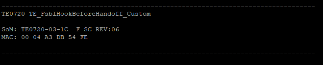
In the FSBL code it must be written the following code additionally. This c file can be found in the following path: \test_board\sw_lib\sw_apps\zynq_fsbl\src\te_fsbl_hooks_te0720.c
For more information refer to TE0720 test board
| Code Block | ||||
|---|---|---|---|---|
| ||||
u32 TE_FsblHookBeforeHandoff_Custom(void)
{
...
Mac_Config = XEmacPs_LookupConfig(XPAR_PS7_ETHERNET_0_DEVICE_ID); if(Mac_Config == NULL) { return XST_FAILURE; }
Status = XEmacPs_CfgInitialize(&Emac, Mac_Config, Mac_Config->BaseAddress); if(Status != XST_SUCCESS){ return XST_FAILURE; }
/*
* Read out MAC Address bytes
*/
Status = XEmacPs_PhyRead(&Emac, 0x1A, 9, &rval16); if(Status != XST_SUCCESS){ return XST_FAILURE; }
mac_addr[0] = (unsigned char)(rval16 >> 8);
mac_addr[1] = (unsigned char)(rval16 & 0xFF);
Status = XEmacPs_PhyRead(&Emac, 0x1A, 10, &rval16); if(Status != XST_SUCCESS){ return XST_FAILURE; }
mac_addr[2] = (unsigned char)(rval16 >> 8);
mac_addr[3] = (unsigned char)(rval16 & 0xFF);
Status = XEmacPs_PhyRead(&Emac, 0x1A, 11, &rval16); if(Status != XST_SUCCESS){ return XST_FAILURE; }
mac_addr[4] = (unsigned char)(rval16 >> 8);
mac_addr[5] = (unsigned char)(rval16 & 0xFF);
...

/*
* Write MAC Address to OCM memory for u-boot to import!
*
*/

//strcpy(0xFFFFFC04, "ethaddr=00:0a:35:00:00:05\n" );
#ifdef UBOOT_ENV_MAGIC
Xil_Out32(UBOOT_ENV_MAGIC_ADDR, UBOOT_ENV_MAGIC); // Magic!
MacToUbootEnvironment((char*)UBOOT_ENV_ADDR, mac_addr);

/*
* Set MAC Address in PS7 IP Core registers
*/
Status = XEmacPs_SetMacAddress(&Emac, mac_addr, 1); if(Status != XST_SUCCESS){ return XST_FAILURE; }
...
} |
Add the following definition in petalinux-configuration platform-top header file:
| Code Block | ||||||
|---|---|---|---|---|---|---|
| ||||||
#define CONFIG_PREBOOT "echo U-BOOT for petalinux;echo importing env from FSBL shared area at 0xFFFFFC00; if itest *0xFFFFFC00 == 0xCAFEBABE; then echo Found valid magic; env import -t 0xFFFFFC04; fi;setenv preboot; echo; dhcp" |
The platform-top.h file can be found in the following path: \petalinux\project-spec\meta-user\recipes-bsp\u-boot\files
The Zynq SoC reads the MAC address from EEPROM by CPLD during power-on and copies this data in OCM (On-chip Memory). After that either in Linux or Uboot console MAC address can be accessed.
Appx. A: Change History and Legal Notices
Revision Changes
- changes REV05 to REV06
Generic options: PUDC and Boot Mode
MIO7 Pullnone
Adding internal en_3v3_int
JTAG C_* high impedance until 3.3VOUT can be high
Boot mode pins are GND or high impedance until en_3v3_int are high
MIO14,15 high impedance until en_3v3_int are high
JTAG time constraint correction
JTAG drive line adjustment
Bugfix I2C to GPIO module (I2C_to_GPIO.v)
- Changed Firmware Identifier to REV06
changes REV04 to REV05:
0.05 watchdog
changes REV03 to REV04:
NA
changes REV02 to REV03:
NA
changes REV01 to REV02:
added deglicht for EN1 and RESIN inputs
added VCORE ON when 3.3 OK signalled
| Scroll Title | ||
|---|---|---|
| ||
|
Document Change History
To get content of older revision got to "Change History" of this page and select older document revision number.
| Page properties | ||||
|---|---|---|---|---|
| ||||
|
Date | Document Revision | CPLD Firmware Revision | Supported PCB Revision | Authors | Description | ||||||||||||||||||||||
|---|---|---|---|---|---|---|---|---|---|---|---|---|---|---|---|---|---|---|---|---|---|---|---|---|---|---|---|
|
| REV06 | REV03, REV02 |
|
| ||||||||||||||||||||||
| 2021-02-03 | v.132 | REV06 | REV03, REV02 | Mohsen Chamanbaz |
| ||||||||||||||||||||||
| 2021-01-29 | v.130 | REV05 | REV03, REV02 | John Hartfiel |
| ||||||||||||||||||||||
| 2021-01-14 | v.127 | REV05 | REV03, REV02 | Mohsen Chamanbaz |
| ||||||||||||||||||||||
All |
|
Legal Notices
| Include Page | ||||
|---|---|---|---|---|
|
| Scroll Only | ||
|---|---|---|
|
| Scroll pdf ignore | ||||||||
|---|---|---|---|---|---|---|---|---|
|
Overview
Content Tools