| Page properties |
|---|
|
- Module: TRM Name always "TE Series Name" +TRM
Example: "TE0728 TRM"
Template Change history: | Date | Version | Changes | Author |
|---|
| 3.12 | - Version History
- changed from list to table
- all
- changed title-alignment for tables from left to center
| ma |
| 3.11 | - update "Recommended Operating Conditions" section
|
|
| 3.1 | - New general notes for temperature range to "Recommended Operating Conditions"
|
|
| 3.02 | - add again fix table of content with workaround to use it for pdf and wiki
- Export Link for key features examples
- Notes for different Types (with and without Main FPGA)
- Export Link for Signals, Interfaces and Pins examples
- Notes for different Types (Modul, Modul Hypride, Evalboard, Carrier)
|
|
| 3.01 | - remove fix table of content and page layout ( split page layout make trouble with pdf export)
- changed and add note to signal and interfaces, to on board periphery section
- ...(not finished)
|
|
| 3.00 | - → separation of Carrier/Module and evaluation kit TRM
|
|
| 2.15 | - add excerpt macro to key features
|
|
| 2.14 | - add fix table of content
- add table size as macro
|
|
|
| Page properties |
|---|
|
Important General Note:
|
| Page properties |
|---|
|
----------------------------------------------------------------------- |
| Page properties |
|---|
|
Note for Download Link of the Scroll ignore macro: |
Overview
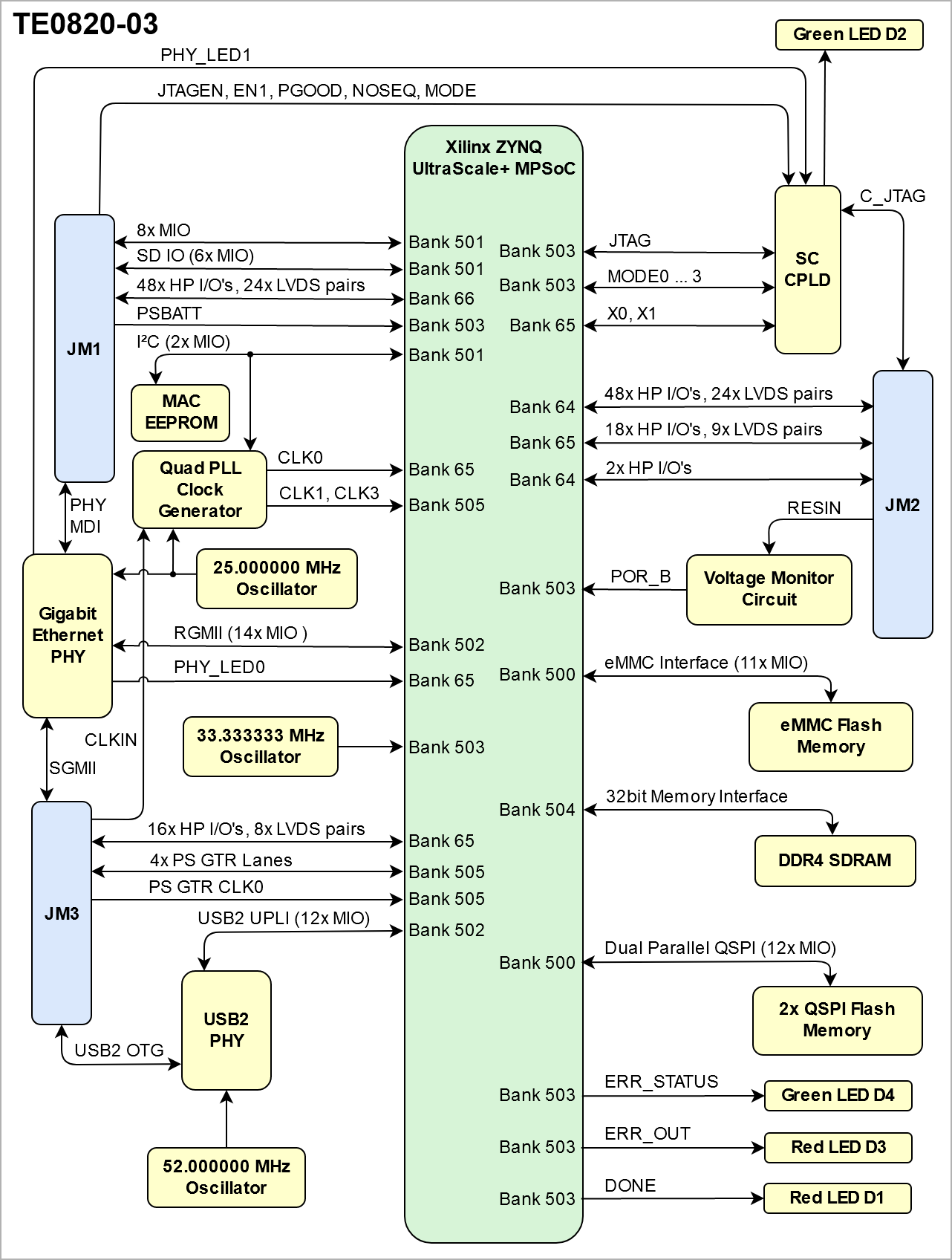
The Trenz Electronic TE0820 is a powerful 4 x 5 cm industrial/extended module integrated with a Xilinx Zynq UltraScale+ MPSoC. In addition, the module is equipped with 2x 8 Gb DDR4 SDRAM chip, up to 64 Gb eMMC chip, 2x 512 Mb flash memory for configuration and data storage, as well as powerful switching power supplies for all required voltages. The module is equipped with a Lattice Mach XO2 CPLD for system controlling. 3x Robust high-speed connectors provide a large number of inputs and outputs. Additionally the module provides Gigabit Ethernet and USB2.0 Transceivers.
The highly integrated modules are smaller than a credit card and are offered in several variants at an affordable price-performance ratio. Modules with a 4 x 5 cm form factor are completely mechanically and largely electrically compatible with each other.
All components cover at least the industrial temperature range. The temperature range in which the module can be used depends on the customer design and the selected cooling. Please contact us for special solutions.
Refer to http://trenz.org/te0820-info for the current online version of this manual and other available documentation.
Key Features
- SoC/FPGA
- Package: SFVC784
- Device: ZU2 ...ZU5, *
- Engine: EG, CG, EV, *
- Speed: -1, -1L, -2, -2L, 3, *, **
- Temperature: I, E, *, **
- RAM/Storage
- 2x DDR4 SDRAM,
- Data Width: 16 Bit
- Size: 8 Gb, *
- Speed: 2400 Mbps, ***
- 2x QSPI boot Flash in dual parallel mode
- Data Width: 8 Bit
- Size: 512 Mb Gb, *
- 1x e.MMC Memory
- Data Width: 16 Bit
- Size: 8 Gb, *
- MAC address serial EEPROM
- On Board
- Lattice MachXO2 CPLD
- Programmable Clock Generator
- Hi-speed USB2 ULPI Transceiver
- 4x LEDS
- Interface
- 1 Gbps RGMII Ethernet interface
- Hi-speed USB2 ULPI transceiver with full OTG support
- Graphic Processor Mali-400 MP2, *
- 156 x High Performance (HP) und 96 x High Density PL I/Os
- 4 x serial PS GTR transceivers
- Power
- All power regulators on board
- Dimension
- Note
- * depends on assembly version
- ** also non low power assembly options possible
- *** depends on used U+ Zynq and DDR4 combination
- Rugged for shock and high vibration
Additional assembly options are available for cost or performance optimization upon request.
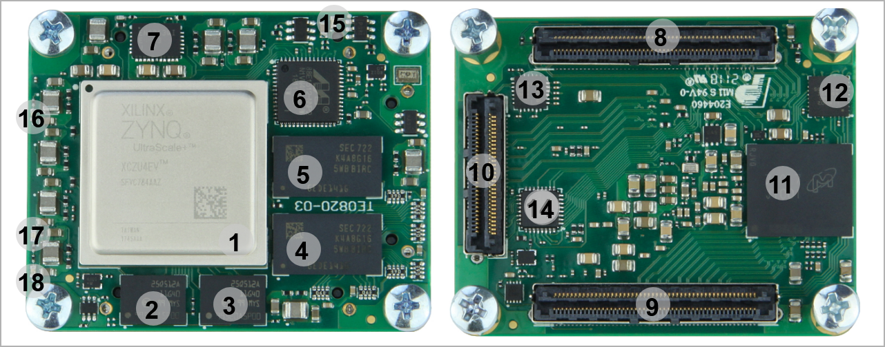
Block Diagram
| Page properties |
|---|
|
add drawIO object in Scroll Ignore section and add reference image in Scroll Only.
| Note |
|---|
Title (not anchor) of all Scroll Title such as DrawIOs and Tables should be changed according to the Module name. Example: TE0812 Block Diagram |
| Note |
|---|
All created DrawIOs should be named according to the Module name: Example: DrawIO of TE0812 Block Diagram should be named TE0812_OV_BD |
|
| Scroll Title |
|---|
| anchor | Figure_OV_BD |
|---|
| title-alignment | center |
|---|
| title | TE0820-03 block diagram |
|---|
|
| Scroll Ignore |
|---|
| draw.io Diagram |
|---|
| border | false |
|---|
| |
|---|
| diagramName | TE0820 BD Block Diagram |
|---|
| simpleViewer | false |
|---|
| width | |
|---|
| links | auto |
|---|
| tbstyle | hidden |
|---|
| diagramDisplayName | |
|---|
| lbox | true |
|---|
| diagramWidth | 641 |
|---|
| revision | 1 |
|---|
|
|
| Scroll Only |
|---|
|
|
Main Components
| Scroll Title |
|---|
| anchor | Figure_OV_MC |
|---|
| title-alignment | center |
|---|
| title | TE0820-03 main components |
|---|
|
| Scroll Ignore |
|---|
| draw.io Diagram |
|---|
| border | false |
|---|
| |
|---|
| diagramName | TE0820 MC main components |
|---|
| simpleViewer | false |
|---|
| width | |
|---|
| links | auto |
|---|
| tbstyle | hidden |
|---|
| diagramDisplayName | |
|---|
| lbox | true |
|---|
| diagramWidth | 641 |
|---|
| revision | 1 |
|---|
|
|
| Scroll Only |
|---|
|
|
- Xilinx Zynq UltraScale+ MPSoC, U1
- 1.8V, 512 Mbit QSPI flash memory, U7
- 1.8V, 512 Mbit QSPI flash memory, U17
- 8 Gbit (512 x 16) DDR4 SDRAM, U2
- 8 Gbit (512 x 16) DDR4 SDRAM, U3
- Marvell Alaska 88E1512 integrated 10/100/1000 Mbps energy efficient ethernet transceiver, U8
- 6A PowerSoC DC-DC converter (PL_VCCINT, 0.85V), U5
- B2B connector Samtec Razor Beam™ LSHM-150, JM1
- B2B connector Samtec Razor Beam™ LSHM-150, JM2
- B2B connector Samtec Razor Beam™ LSHM-130, JM3
- 8 GByte eMMC memory, U6
- Lattice Semiconductor MachXO2 System Controller CPLD, U21
- I2C programmable, any frequency , any output quad clock generator, U10
- Highly integrated full featured hi-speed USB 2.0 ULPItransceiver, U18
- LED D1(Red) Done Pin
- LED D2 (Green) CPLD Status, User LED
- LED D3 (Red) PS Error
- LED D4 (Green) PS Error Status
Initial Delivery State
| Page properties |
|---|
|
| Note |
|---|
Only components like EEPROM, QSPI flash can be initialized by default at manufacture. If there is no components which might have initial data ( possible on carrier) you must keep the table empty |
|
| Scroll Title |
|---|
| anchor | Table_OV_IDS |
|---|
| title-alignment | center |
|---|
| title | Initial delivery state of programmable devices on the module |
|---|
|
| Scroll Table Layout |
|---|
| orientation | portrait |
|---|
| sortDirection | ASC |
|---|
| repeatTableHeaders | default |
|---|
| style | |
|---|
| widths | |
|---|
| sortByColumn | 1 |
|---|
| sortEnabled | false |
|---|
| cellHighlighting | true |
|---|
|
Storage device name | Content | Notes |
|---|
Dual QSPI Flash Memory | Not programmed |
| eMMC Memory | Not programmed |
| | DDR4 SDRAM | Not programmed |
| | Programmable Clock Generator | Not programmed |
| | CPLD (LCMXO2-256HC) | Programmed | TE0820 CPLD |
|
Configuration Signals
| Page properties |
|---|
|
- Overview of Boot Mode, Reset, Enables.
|
Two different firmware versions are available, one with the QSPI boot option and other with the SD Card boot option.
| Scroll Title |
|---|
| anchor | Table_OV_BP |
|---|
| title-alignment | center |
|---|
| title | Boot process. |
|---|
|
| Scroll Table Layout |
|---|
| orientation | portrait |
|---|
| sortDirection | ASC |
|---|
| repeatTableHeaders | default |
|---|
| style | |
|---|
| widths | |
|---|
| sortByColumn | 1 |
|---|
| sortEnabled | false |
|---|
| cellHighlighting | true |
|---|
|
MODE Pin | Boot Mode |
|---|
| Low | QSPI | | High | SD Card |
|
| Scroll Title |
|---|
| anchor | Table_OV_RST |
|---|
| title-alignment | center |
|---|
| title | Reset process. |
|---|
|
| Scroll Table Layout |
|---|
| orientation | portrait |
|---|
| sortDirection | ASC |
|---|
| repeatTableHeaders | default |
|---|
| style | |
|---|
| widths | |
|---|
| sortByColumn | 1 |
|---|
| sortEnabled | false |
|---|
| cellHighlighting | true |
|---|
|
Signal | B2B | I/O | Note |
|---|
EN1 | JM1-28 | Input | CPLD Enable Pin | | RESIN | JM2-18 | Input | General Reset |
|
Signals, Interfaces and Pins
Board to Board (B2B) I/Os
Zynq MPSoC's I/O banks signals connected to the B2B connectors:
| Scroll Title |
|---|
| anchor | Table_SIP_B2B |
|---|
| title-alignment | center |
|---|
| title | General PL I/O to B2B connectors information |
|---|
|
| Scroll Table Layout |
|---|
| orientation | portrait |
|---|
| sortDirection | ASC |
|---|
| repeatTableHeaders | default |
|---|
| style | |
|---|
| widths | |
|---|
| sortByColumn | 1 |
|---|
| sortEnabled | false |
|---|
| cellHighlighting | true |
|---|
|
| Bank | Type | B2B Connector | I/O Signal Count | Voltage | Notes |
|---|
64 | HP | JM2 | 48x Single Ended, 24x LVDS Pairs | Variable | Max voltage 1.8V | 64 | HP | JM2 | 2x Single Ended | Variable | Max voltage 1.8V | | 65 | HP | JM2 | 18x Single Ended, 9x LVDS Pairs | Variable | Max voltage 1.8V | 65 | HP | JM3 | 16x Single Ended, 8x LVDS Pairs | Variable | Max voltage 1.8V | 66 | HP | JM1 | 48x Single Ended, 24x LVDS Pairs | Variable | Max voltage 1.8V | | 500 | MIO | JM1 | 8x Single Ended | 1.8V |
| 501 | MIO | JM1 | 6x Single Ended | 3.3V |
| 505 | GTR | JM3 | 16x Single Ended, 8x LVDS Pairs | - | 4x Lanes | 505 | GTR CLK | JM3 | 1x differential Clock | - |
|
|
For detailed information about the pin-out, please refer to the Pin-out table.
MGT Lanes
The Xilinx Zynq UltraScale+ device used on the TE0820 module has 4 GTR transceivers. All 4 are wired directly to B2B connector JM3. MGT (Multi Gigabit Transceiver) lane consists of one transmit and one receive (TX/RX) differential pairs, four signals total per one MGT lane. Following table lists lane number, FPGA bank number, transceiver type, signal schematic name, board-to-board pin connection and FPGA pins connection:
| Scroll Title |
|---|
| anchor | Table_SIP_MGT |
|---|
| title-alignment | center |
|---|
| title | MGT Lanes connection |
|---|
|
| Scroll Table Layout |
|---|
| orientation | portrait |
|---|
| sortDirection | ASC |
|---|
| repeatTableHeaders | default |
|---|
| style | |
|---|
| widths | |
|---|
| sortByColumn | 1 |
|---|
| sortEnabled | false |
|---|
| cellHighlighting | true |
|---|
|
| Lane | Bank | Signal Name | B2B Pin | Note |
|---|
| 0 | 505 | - B505_RX0_P
- B505_RX0_N
- B505_TX0_P
- B505_TX0_N
| |
| | 1 | 505 | - B505_RX1_P
- B505_RX1_N
- B505_TX1_P
- B505_TX1_N
| |
| | 2 | 505 | - B505_RX2_P
- B505_RX2_N
- B505_TX2_P
- B505_TX2_N
| |
| | 3 | 505 | - B505_RX3_P
- B505_RX3_N
- B505_TX3_P
- B505_TX3_N
| |
|
|
There are 3 clock sources for the GTR transceivers. B505_CLK0 is connected directly to B2B connector JM3, so the clock can be provided by the carrier board. Clocks B505_CLK1 and B505_CLK3 are provided by the on-board clock generator (U10). As there are no capacitive coupling of the data and clock lines that are connected to the connectors, these may be required on the user’s PCB depending on the application.
| Scroll Title |
|---|
| anchor | Table_SIP_MGTCLK |
|---|
| title-alignment | center |
|---|
| title | MGT Clock Sources Information |
|---|
|
| Scroll Table Layout |
|---|
| orientation | portrait |
|---|
| sortDirection | ASC |
|---|
| repeatTableHeaders | default |
|---|
| style | |
|---|
| widths | |
|---|
| sortByColumn | 1 |
|---|
| sortEnabled | false |
|---|
| cellHighlighting | true |
|---|
|
| Clock signal | Bank | Connected to | Notes |
|---|
| B505_CLK0_P | 505 | B2B, JM3-31 | Supplied by the carrier board | | B505_CLK0_N | 505 | B2B, JM3-33 | Supplied by the carrier board | | B505_CLK1_P | 505 | U10, CLK2A | On-board Si5338A | | B505_CLK1_N | 505 | U10, CLK2B | On-board Si5338A | | B505_CLK2_P | 505 | N/A | Not connected | | B505_CLK2_N | 505 | N/A | Not connected | | B505_CLK3_P | 505 | U10, CLK1A | On-board Si5338A | | B505_CLK3_N | 505 | U10, CLK1B | On-board Si5338A |
|
JTAG Interface
JTAG access to the Xilinx Zynq-7000 is provided through B2B connector JM2.
| Scroll Title |
|---|
| anchor | Table_SIP_JTG |
|---|
| title-alignment | center |
|---|
| title | JTAG pins connection |
|---|
|
| Scroll Table Layout |
|---|
| orientation | portrait |
|---|
| sortDirection | ASC |
|---|
| repeatTableHeaders | default |
|---|
| style | |
|---|
| widths | |
|---|
| sortByColumn | 1 |
|---|
| sortEnabled | false |
|---|
| cellHighlighting | true |
|---|
|
JTAG Signal | B2B Connector Pin | Notes |
|---|
| TMS | JM2-93 |
| | TDI | JM2-95 |
| | TDO | JM2-97 |
| | TCK | JM2-99 |
| | JTAGEN | JM1-89 | Pulled Low: Xilinx Zynq UltraScale+ MPSoC
Pulled High: Lattice MachXO CPLD |
|
Pin 89 JTAGEN of B2B connector JM1 is used to control which device is accessible via JTAG. If set to low or grounded, JTAG interface will be routed to the Xilinx Zynq MPSoC. If pulled high, JTAG interface will be routed to the System Controller CPLD.
I2C Addresses
On-board I2C devices are connected to MIO38 (SCL) and MIO39 (SDA) which are configured as I2C0 by default. Addresses for on-board I2C slave devices are listed in the table below:
| Scroll Title |
|---|
| anchor | Table_SIP_I2C |
|---|
| title-alignment | center |
|---|
| title | Address table of the I2C bus slave devices |
|---|
|
| Scroll Table Layout |
|---|
| orientation | portrait |
|---|
| sortDirection | ASC |
|---|
| repeatTableHeaders | default |
|---|
| style | |
|---|
| widths | |
|---|
| sortByColumn | 1 |
|---|
| sortEnabled | false |
|---|
| cellHighlighting | true |
|---|
|
| I2C Device | I2C Address | Notes |
|---|
PLL Clock Generator, U10 | 0x70/ 0x71 |
| | EEPROM, U25 | 0x50 |
|
|
MIOs
| Scroll Title |
|---|
| anchor | Table_SIP_MIOs |
|---|
| title-alignment | center |
|---|
| title | MIOs pins |
|---|
|
| Scroll Table Layout |
|---|
| orientation | portrait |
|---|
| sortDirection | ASC |
|---|
| repeatTableHeaders | default |
|---|
| style | |
|---|
| widths | |
|---|
| sortByColumn | 1 |
|---|
| sortEnabled | false |
|---|
| cellHighlighting | true |
|---|
|
| MIO Pin | Connected to | B2B | Notes |
|---|
| 0...5 | QSPI Flash, U7 | - | SPI Flash | | 7...12 | QSPI Flash, U17 | - | SPI Flash | | 13...23 | eMMC, U6 |
| eMMC | | 24 | ETH Transceiver, U8 | - | ETH_RST | | 25 | USB2.0 Transceiver, U18 | - | OTG_RST | | 26...33 | User MIO | JM1 |
| | 34...37 | N.C | - | N.C | | 38...39 | EEPROM, U25 | - | I2C_SDA/SCL | | 40...45 | N.C |
| N.C | | 46...51 | SD Card | JM1 |
| | 52...63 | USB2.0 Transceiver, U18 | - |
| | 63...77 | Ethernet Transceiver, U8 | - |
|
|
Test Points
| Scroll Title |
|---|
| anchor | Table_SIP_TPs |
|---|
| title-alignment | center |
|---|
| title | Test Points Information |
|---|
|
| Scroll Table Layout |
|---|
| orientation | portrait |
|---|
| sortDirection | ASC |
|---|
| repeatTableHeaders | default |
|---|
| style | |
|---|
| widths | |
|---|
| sortByColumn | 1 |
|---|
| sortEnabled | false |
|---|
| cellHighlighting | true |
|---|
|
| Test Point | Signal | Connected to | Notes |
|---|
| 1 | PS_LP0V85 | Voltage Regulator, U12 |
| | 2 | DDR_2V5 | Voltage Regulator, U4 |
| | 3 | PS_AVCC | Voltage Regulator, U9 |
| | 4 | DDR_1V2 | Voltage Regulator, U15 |
| | 5 | PS_AVTT | Voltage Regulator, U3 |
| | 6 | VTT | Regulator, U16 |
| | 7 | PS_FP0V85 | Voltage Regulator, U26 |
| | 8 | VREFA | Regulator, U16 |
| | 10 | PS_PLL | Voltage Regulator, U23 |
| | 11 | PL_VCCINT | Voltage Regulator, U5 |
| | 15 | PL_VCCINT_IO | Voltage Regulator, U27 |
| | 16 | PL_VCU | Voltage Regulator, U24 |
|
|
On-board Peripherals
| Page properties |
|---|
|
Notes : In the on-board peripheral table "chip/Interface" must be linked to the corresponding chapter or subsection by assigning advance link using: #NameOfTheSection Example: #ClockSources, #CPLD, #QuadSPIFlash |
| Scroll Title |
|---|
| anchor | Table_OBP |
|---|
| title-alignment | center |
|---|
| title | On board peripherals |
|---|
|
| Scroll Table Layout |
|---|
| orientation | portrait |
|---|
| sortDirection | ASC |
|---|
| repeatTableHeaders | default |
|---|
| style | |
|---|
| widths | |
|---|
| sortByColumn | 1 |
|---|
| sortEnabled | false |
|---|
| cellHighlighting | true |
|---|
|
|
System Controller CPLD
The System Controller CPLD (U21) is provided by Lattice Semiconductor LCMXO2-256HC (MachXO2 product family). It is the central system management unit with module specific firmware installed to monitor and control various signals of the FPGA, on-board peripherals, I/O interfaces and module.
Special purpose pins are connected to System Controller CPLD and have following default configuration:
| Scroll Title |
|---|
| anchor | Table_SIP_CPLD |
|---|
| title-alignment | center |
|---|
| title | System Controller CPLD special purpose pins |
|---|
|
| Scroll Table Layout |
|---|
| orientation | portrait |
|---|
| sortDirection | ASC |
|---|
| repeatTableHeaders | default |
|---|
| style | |
|---|
| widths | |
|---|
| sortByColumn | 1 |
|---|
| sortEnabled | false |
|---|
| cellHighlighting | true |
|---|
|
| Pin Name | Mode | Function | Default Configuration |
|---|
| EN1 | Input | Power Enable | No hard wired function on PCB. When forced low, PGOOD goes low without effect on power management | | PGOOD | Output | Power Good | Only indirect used for power status, see CPLD description | | NOSEQ | - | - | No used for Power sequencing, see CPLD description | | RESIN | Input | Reset | Active low reset, gated to POR_B | | JTAGEN | Input | JTAG Select | Low for normal operation, high for CPLD JTAG access |
|
Please check the entire information at TE0820 CPLD.
See also TE0820 System Controller CPLD page.
eMMC Memory
eMMC Flash memory device(U6) is connected to the ZynqMP PS MIO bank 500 pins MIO13..MIO23. eMMC chips IS21ES08G-JCLI (FLASH - NAND Speicher-IC (64 Gb x 1) MMC ) is used.
DDR4 Memory
The TE0820 SoM has dual 8 Gb volatile DDR4 SDRAM IC for storing user application code and data.
- Part number: K4A8G165WB-BIRC
- Supply voltage: 1.2V
- Speed: 2400 Mbps
- Temperature: -40 ~ 95 °C
Quad SPI Flash Memory
Two quad SPI compatible serial bus flash MT25QU512ABB8E12-0SIT memory chips are provided for FPGA configuration file storage. After configuration completes the remaining free memory can be used for application data storage. All four SPI data lines are connected to the FPGA allowing x1, x2 or x4 data bus widths to be used. The maximum data transfer rate depends on the bus width and clock frequency.
Gigabit Ethernet
On-board Gigabit Ethernet PHY (U8) is provided with Marvell Alaska 88E1512 IC (U8). The Ethernet PHY RGMII interface is connected to the ZynqMP Ethernet3 PS GEM3. I/O voltage is fixed at 1.8V for HSTL signaling. The reference clock input of the PHY is supplied from an on-board 25.000000 MHz oscillator (U11).
High-speed USB ULPI PHY
| Scroll Title |
|---|
| anchor | Table_SIP_ETH |
|---|
| title-alignment | center |
|---|
| title | GigaBit Ethernet connection |
|---|
|
| Scroll Table Layout |
|---|
| orientation | portrait |
|---|
| sortDirection | ASC |
|---|
| repeatTableHeaders | default |
|---|
| style | |
|---|
| widths | |
|---|
| sortByColumn | 1 |
|---|
| sortEnabled | false |
|---|
| cellHighlighting | true |
|---|
|
| Pin | Schematic | Connected to | Note |
|---|
| MDIP0...3 | PHY_MDI0...3 | B2B, JM1 |
| | MDC | ETH_MDC | MIO76 |
| | MDIO | ETH_MDIO | MIO77 |
| | S_IN | S_IN | B2B, JM3 |
| | S_OUT | S_OUT | B2B, JM3 |
| | TXD0..3 | ETH_TXD0...3 | MIO65...68 |
| | TX_CTRL | ETH_TXCTL | MIO69 |
| | TX_CLK | ETH_TXCK | MIO64 |
| | RXD0...3 | ETH_RXD0...3 | MIO71...74 |
| | RX_CTRL | ETH_RXCTL | MIO75 |
| | RX_CLK | ETH_RXCK | MIO70 |
| | LED1 | PHY_LED1 | CPLD, U21 |
| | RESETn | ETH_RST | MIO24 |
|
|
USB2.0 Transceiver
Hi-speed USB ULPI PHY (U18) is provided with USB3320 from Microchip. The ULPI interface is connected to the Zynq PS USB0 via MIO52..63, bank 502. The I/O voltage is fixed at 1.8V and PHY reference clock input is supplied from the on-board 52.00 MHz oscillator (U14).
| Scroll Title |
|---|
| anchor | Table_SIP_USB |
|---|
| title-alignment | center |
|---|
| title | General overview of the USB PHY signals |
|---|
|
| Scroll Table Layout |
|---|
| orientation | portrait |
|---|
| sortDirection | ASC |
|---|
| repeatTableHeaders | default |
|---|
| style | |
|---|
| widths | |
|---|
| sortByColumn | 1 |
|---|
| sortEnabled | false |
|---|
| cellHighlighting | true |
|---|
|
| PHY Pin | ZYNQ Pin | B2B Name | Notes |
|---|
| ULPI | MIO52..63 | - | Zynq USB0 MIO pins are connected to the USB PHY. | | REFCLK | - | - | 52.000000 MHz from on-board oscillator (U14). | | REFSEL[0..2] | - | - | Reference clock frequency select, all set to GND selects 52.000000 MHz. | | RESETB | MIO25 | - | Active low reset. | | CLKOUT | MIO52 | - | Connected to 1.8V, selects reference clock operation mode. | | DP, DM | - | OTG_D_P, OTG_D_N | USB data lines routed to B2B connector JM3 pins 47 and 49. | | CPEN | - | VBUS_V_EN | External USB power switch active high enable signal, routed to JM3 pin 17. | | VBUS | - | USB_VBUS | Connect to USB VBUS via a series of resistors, see reference schematics, routed to JM3 pin 55. | | ID | - | OTG_ID | For an A-device connect to ground, for a B-device left floating. routed from JM3 pin 23. |
|
EEPROM
There is a 2Kb EEPROM (U25) provided on the module TE0820.
| Scroll Title |
|---|
| anchor | Table_OBP_EEP |
|---|
| title-alignment | center |
|---|
| title | I2C EEPROM interface MIOs and pins |
|---|
|
| Scroll Table Layout |
|---|
| orientation | portrait |
|---|
| sortDirection | ASC |
|---|
| repeatTableHeaders | default |
|---|
| style | |
|---|
| widths | |
|---|
| sortByColumn | 1 |
|---|
| sortEnabled | false |
|---|
| cellHighlighting | true |
|---|
|
| MIO Pin | Schematic | U25 Pin | Notes |
|---|
| MIO39 | I2C_SDA | SDA |
| | MIO38 | I2C_SCL | SCL |
|
|
Programmable Clock Generator
There is a Silicon Labs I2C programmable clock generator Si5338A (U10) chip on the module. It's output frequencies can be programmed using the I2C bus address 0x70 or 0x71. Default address is 0x70, IN4/I2C_LSB pin must be set to high for address 0x71.
A 25.000000 MHz oscillator is connected to the pin IN3 and is used to generate the output clocks. The oscillator has its output enable pin permanently connected to 1.8V power rail, thus making output frequency available as soon as 1.8V is present. Three of the Si5338 clock outputs are connected to the FPGA. One is connected to a logic bank and the other two are connected to the GTR banks.
Once running, the frequency and other parameters can be changed by programming the device using the I2C bus connected between the FPGA (master) and clock generator (slave). For this, proper I2C bus logic has to be implemented in FPGA.
| Scroll Title |
|---|
| anchor | Table_OBP_PCLK |
|---|
| title-alignment | center |
|---|
| title | Programmable Clock Generator Inputs and Outputs |
|---|
|
| Scroll Table Layout |
|---|
| orientation | portrait |
|---|
| sortDirection | ASC |
|---|
| repeatTableHeaders | default |
|---|
| sortByColumn | 1 |
|---|
| sortEnabled | false |
|---|
| cellHighlighting | true |
|---|
|
| U25 Pin | Signal | Connected to | Direction | Note |
|---|
IN0..1 | CLK_IN | JM3 | IN |
| | IN2 | CLK_25M | Oscillator, U11 | IN |
| | SCL | I2C_SCL | EEPROM,U25 | INOUT |
| | SDA | I2C_SDA | EEPROM,U25 | INOUT |
| | CLK0 | CLK0 | JM3 | OUT |
| | CLK1 | B505_CLK3 | FPGA Bank 505 | IN |
| | CLK2 | B505_CLK1 | FPGA Bank 505 | IN |
| | CLK3 | CLK3_N |
| IN |
|
|
Clock Sources
| Scroll Title |
|---|
| anchor | Table_OBP_CLK |
|---|
| title-alignment | center |
|---|
| title | Osillators |
|---|
|
| Scroll Table Layout |
|---|
| orientation | portrait |
|---|
| sortDirection | ASC |
|---|
| repeatTableHeaders | default |
|---|
| style | |
|---|
| widths | |
|---|
| sortByColumn | 1 |
|---|
| sortEnabled | false |
|---|
| cellHighlighting | true |
|---|
|
| Designator | Description | Frequency | Clock Destination |
|---|
| U32 | MEMS Oscillator | 33.33 MHz |
| | U11 | MEMS Oscillator | 25 MHz |
| | U14 | MEMS Oscillator | 52 MHz |
|
|
LEDs
| Scroll Title |
|---|
| anchor | Table_OBP_LED |
|---|
| title-alignment | center |
|---|
| title | On-board LEDs |
|---|
|
| Scroll Table Layout |
|---|
| orientation | portrait |
|---|
| sortDirection | ASC |
|---|
| repeatTableHeaders | default |
|---|
| style | |
|---|
| widths | |
|---|
| sortByColumn | 1 |
|---|
| sortEnabled | false |
|---|
| cellHighlighting | true |
|---|
|
| Designator | Color | Connected to | Active Level | Note |
|---|
| D1 | Red | DONE | Low |
| | D2 | Green | USR_LED | High |
| | D3 | Red | ERR_OUT | High |
| | D4 | Green | ERR_STATUS | High |
|
|
Power and Power-on Sequence
| Page properties |
|---|
|
In 'Power and Power-on Sequence' section there are three important digrams which must be drawn: - Power on-sequence
- Power distribution
- Voltage monitoring circuit
|
Power Supply
Power supply with minimum current capability of 3A for system startup is recommended.
Power Consumption
| Scroll Title |
|---|
| anchor | Table_PWR_PC |
|---|
| title-alignment | center |
|---|
| title | Power Consumption |
|---|
|
| Scroll Table Layout |
|---|
| orientation | portrait |
|---|
| sortDirection | ASC |
|---|
| repeatTableHeaders | default |
|---|
| style | |
|---|
| widths | |
|---|
| sortByColumn | 1 |
|---|
| sortEnabled | false |
|---|
| cellHighlighting | true |
|---|
|
| Power Input Pin | Typical Current |
|---|
| VIN | TBD* | | 3.3VIN | TBD* |
|
* TBD - To Be Determined soon with reference design setup.
For the lowest power consumption and highest efficiency of the on-board DC-DC regulators it is recommended to power the module from one single 3.3V supply. All input power supplies should have a nominal value of 3.3V. Although the input power supplies can be powered up in any order, it is recommended to power them up simultaneously.
| Warning |
|---|
| To avoid any damage to the module, check for stabilized on-board voltages should be carried out (i.e. power good and enable signals) before powering up any Zynq's I/O bank voltages VCCO_x. All I/Os should be tri-stated during power-on sequence. |
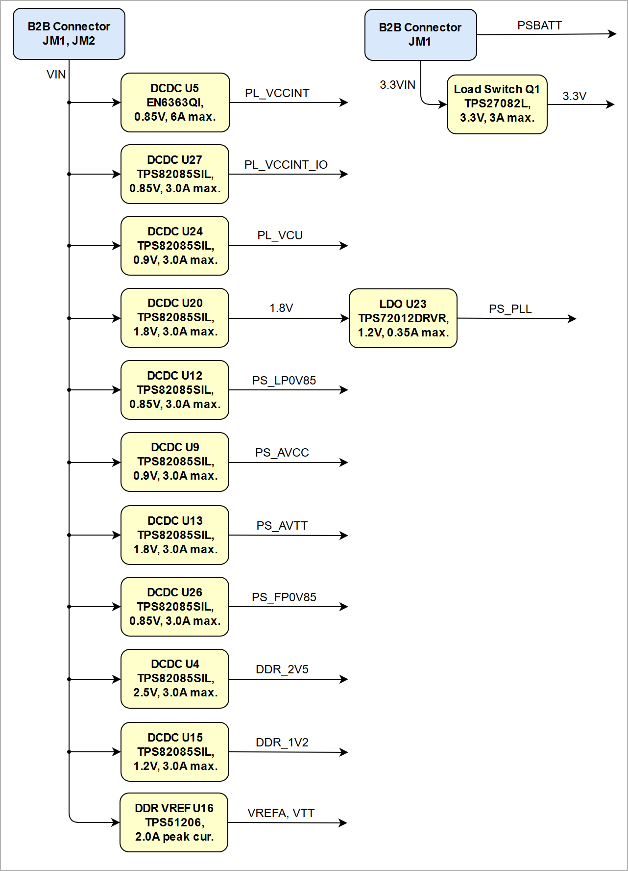
Power Distribution Dependencies
| Scroll Title |
|---|
| anchor | Figure_3 |
|---|
| title-alignment | center |
|---|
| title | Figure 3: TE0820-03 Power Distribution Diagram |
|---|
|
| Scroll Ignore |
|---|
| draw.io Diagram |
|---|
| border | false |
|---|
| |
|---|
| diagramName | TE0820 power dd distribution diagram |
|---|
| simpleViewer | false |
|---|
| width | |
|---|
| links | auto |
|---|
| tbstyle | hidden |
|---|
| diagramDisplayName | |
|---|
| lbox | true |
|---|
| diagramWidth | 641 |
|---|
| revision | 1 |
|---|
|
|
| Scroll Only |
|---|
|
|
See also Xilinx datasheet DS925 for additional information. User should also check related base board documentation when intending base board design for TE0820 module.
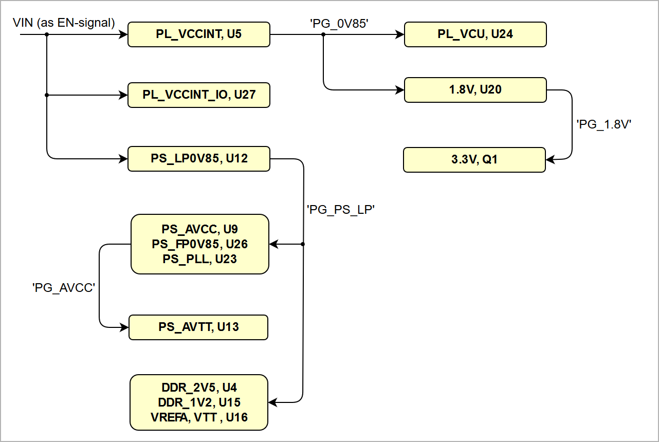
Power-On Sequence
The TE0820 SoM keeping a specific sequence of enabling the on-board DC-DC converters dedicated to the particular functional units of the Zynq chip and powering up the on-board voltages.
Following diagram clarifies the sequence of enabling the particular on-board voltages, which will power-up in descending order as listed in the blocks of the diagram:
| Scroll Title |
|---|
| anchor | Figure_4 |
|---|
| title-alignment | center |
|---|
| title | Figure 4: TE0820-03 Power-on Sequence Diagram |
|---|
|
| Scroll Ignore |
|---|
| draw.io Diagram |
|---|
| border | false |
|---|
| |
|---|
| diagramName | TE0820 PS Power-on Sequence |
|---|
| simpleViewer | false |
|---|
| width | |
|---|
| links | auto |
|---|
| tbstyle | hidden |
|---|
| diagramDisplayName | |
|---|
| lbox | true |
|---|
| diagramWidth | 641 |
|---|
| revision | 1 |
|---|
|
|
| Scroll Only |
|---|
|
|
For highest efficiency of the on-board DC-DC regulators, it is recommended to use one 3.3V power source for both VIN and 3.3VIN power rails. Although VIN and 3.3VIN can be powered up in any order, it is recommended to power them up simultaneously.
It is important that all carrier board I/Os are 3-stated at power-on until 3.3V_out or 1.8V_out is present on B2B connector JM2 pins 10 and 12, indicating that all on-module voltages have become stable and module is properly powered up.
See Xilinx datasheet DS925 for additional information. User should also check related carrier board documentation when choosing carrier board design for TE0715 module.
Power Rails
| Scroll Title |
|---|
| anchor | Table_PWR_PR |
|---|
| title-alignment | center |
|---|
| title | Module power rails. |
|---|
|
| Scroll Table Layout |
|---|
| orientation | portrait |
|---|
| sortDirection | ASC |
|---|
| repeatTableHeaders | default |
|---|
| style | |
|---|
| widths | |
|---|
| sortByColumn | 1 |
|---|
| sortEnabled | false |
|---|
| cellHighlighting | true |
|---|
|
| Power Rail Name on B2B Connector | JM1 Pins | JM2 Pins | Direction | Notes |
|---|
| VIN | 1, 3, 5 | 2, 4, 6, 8 | Input | Supply voltage from the carrier board | | 3.3V | - | 10, 12 | Output | Internal 3.3V voltage level | | 3.3VIN | 13, 15 | - | Input | Supply voltage from the carrier board | | 1.8V | 39 | - | Output | Internal 1.8V voltage level | | JTAG VREF | - | 91 | Output | JTAG reference voltage.
Attention: Net name on schematic is "3.3VIN" | | VCCO_64 | - | 7, 9 | Input | High performance I/O bank voltage | | VCCO_65 | - | 5 | Input | High performance I/O bank voltage | | VCCO_66 | 9, 11 | - | Input | High performance I/O bank voltage |
|
Bank Voltages
| Scroll Title |
|---|
| anchor | Table_PWR_BV |
|---|
| title-alignment | center |
|---|
| title | Zynq SoC bank voltages. |
|---|
|
| Scroll Table Layout |
|---|
| orientation | portrait |
|---|
| sortDirection | ASC |
|---|
| repeatTableHeaders | default |
|---|
| style | |
|---|
| widths | |
|---|
| sortByColumn | 1 |
|---|
| sortEnabled | false |
|---|
| cellHighlighting | true |
|---|
|
| FPGA Bank | Schematic | Voltage | Note |
|---|
| Bank 24 HD | VCCO_HD24_24 | Variable | Max voltage 3.3V | | Bank 25 HD |
| Variable | Max voltage 3.3V | | Bank 26 HD | VCCO_HD25_26 | Variable | Max voltage 3.3V | | Bank 44 HD | VCCO_HD24_44 | Variable | Max voltage 3.3V | | Bank 64 HP | VCCO_64 | N.C | Not Connected | | Bank 65 HP | VCCO_65 | Variable | Max voltage 1.8V | | Bank 66 HP | VCCO_66 | 1.8V |
| | Bank 500 PSMIO | VCCO_PSIO0_500 | 1.8V |
| Bank 501 PSMIO | VCCO_PSIO1_501 | 3.3V |
| | Bank 502 PSMIO | VCCO_PSIO2_502 | 1.8V |
| | Bank 503 PSCONFIG | VCCO_PSIO3_503 | 1.8V |
| | Bank 504 PSDDR | DDR_1V2 | 1.2V |
|
|
Board to Board Connectors
| Page properties |
|---|
|
- This section is optional and only for modules.
use "include page" macro and link to the general B2B connector page of the module series, For example: 6 x 6 SoM LSHM B2B Connectors
| Include Page |
|---|
| 6 x 6 SoM LSHM B2B Connectors |
|---|
| 6 x 6 SoM LSHM B2B Connectors |
|---|
|
|
| Include Page |
|---|
| 4 x 5 SoM LSHM B2B Connectors |
|---|
| 4 x 5 SoM LSHM B2B Connectors |
|---|
|
Technical Specifications
Absolute Maximum Ratings
| Scroll Title |
|---|
| anchor | Table_TS_AMR |
|---|
| title-alignment | center |
|---|
| title | PS absolute maximum ratings |
|---|
|
| Scroll Table Layout |
|---|
| orientation | portrait |
|---|
| sortDirection | ASC |
|---|
| repeatTableHeaders | default |
|---|
| style | |
|---|
| widths | |
|---|
| sortByColumn | 1 |
|---|
| sortEnabled | false |
|---|
| cellHighlighting | true |
|---|
|
Parameter | Min | Max | Units | Notes |
|---|
VIN supply voltage | -0.3 | 7 | V | See EN6347QI and TPS82085SIL datasheets | | 3.3VIN supply voltage | -0.1 | 3.630 | V | Xilinx DS925 and TPS27082L datasheet | | PS I/O supply voltage, VCCO_PSIO | -0.5 | 3.630 | V | Xilinx document DS925 | | PS I/O input voltage | -0.5 | VCCO_PSIO + 0.55 | V | Xilinx document DS925 | | HP I/O bank supply voltage, VCCO | -0.5 | 2.0 | V | Xilinx document DS925 | | HP I/O bank input voltage | -0.55 | VCCO + 0.55 | V | Xilinx document DS925 | | PS GTR reference clocks absolute input voltage | -0.5 | 1.1 | V | Xilinx document DS925 | | PS GTR absolute input voltage | -0.5 | 1.1 | V | Xilinx document DS925 | Voltage on SC CPLD pins | -0.5 | 3.75 | V | Lattice Semiconductor MachXO2 datasheet | Storage temperature | -40 | +85 | °C | See eMMC datasheet |
|
Recommended Operating Conditions
| Scroll Title |
|---|
| anchor | Table_TS_ROC |
|---|
| title-alignment | center |
|---|
| title | Recommended operating conditions. |
|---|
|
| Scroll Table Layout |
|---|
| orientation | portrait |
|---|
| sortDirection | ASC |
|---|
| repeatTableHeaders | default |
|---|
| style | |
|---|
| widths | |
|---|
| sortByColumn | 1 |
|---|
| sortEnabled | false |
|---|
| cellHighlighting | true |
|---|
|
| Parameter | Min | Max | Units | Notes |
|---|
| VIN supply voltage | 3.3 | 6 | V | See TPS82085S datasheet | | 3.3VIN supply voltage | 3.3 | 3.465 | V | See LCMXO2-256HC, Xilinx DS925 datasheet | | PS I/O supply voltage, VCCO_PSIO | 1.710 | 3.465 | V | Xilinx document DS925 | | PS I/O input voltage | –0.20 | VCCO_PSIO + 0.20 | V | Xilinx document DS925 | | HP I/O banks supply voltage, VCCO | 0.950 | 1.9 | V | Xilinx document DS925 | | HP I/O banks input voltage | -0.20 | VCCO + 0.20 | V | Xilinx document DS925 | | Voltage on SC CPLD pins | -0.3 | 3.6 | V | Lattice Semiconductor MachXO2 datasheet | | Operating Temperature Range | 0 | 85 | °C | Xilinx document DS925, extended grade Zynq temperarure range |
|
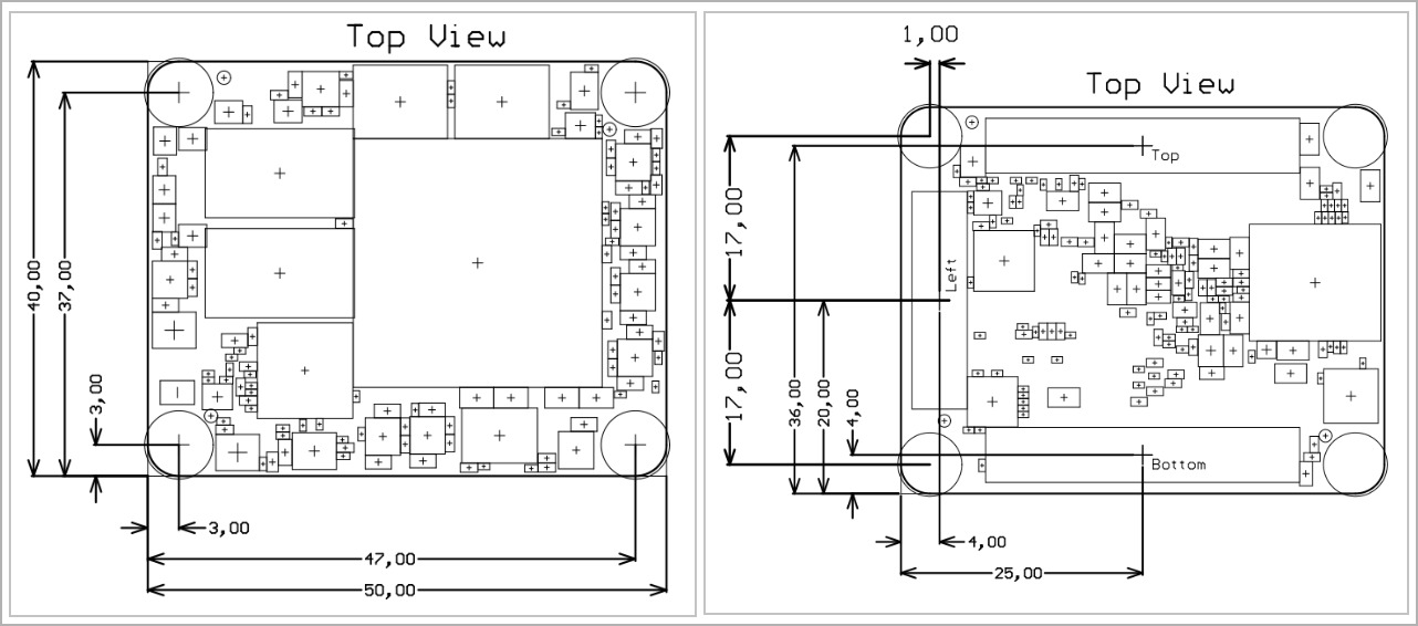
Physical Dimensions
Module size: 50 mm × 40 mm. Please download the assembly diagram for exact numbers.
Mating height with standard connectors: 8 mm
PCB thickness: 1.6 mm
Highest part on PCB: approximately 5 mm. Please download the step model for exact numbers.
All dimensions are shown in millimeters.
| Scroll Title |
|---|
| anchor | Figure_TS_PD |
|---|
| title-alignment | center |
|---|
| title | Physical Dimension |
|---|
|
| Scroll Ignore |
|---|
| draw.io Diagram |
|---|
| border | false |
|---|
| |
|---|
| diagramName | TE0820_TS_PD PD |
|---|
| simpleViewer | false |
|---|
| width | |
|---|
| links | auto |
|---|
| tbstyle | hidden |
|---|
| diagramDisplayName | |
|---|
| lbox | true |
|---|
| diagramWidth | 641 |
|---|
| revision | 1 |
|---|
|
|
| Scroll Only |
|---|
| scroll-pdf | true |
|---|
| scroll-office | true |
|---|
| scroll-chm | true |
|---|
| scroll-docbook | true |
|---|
| scroll-eclipsehelp | true |
|---|
| scroll-epub | true |
|---|
| scroll-html | true |
|---|
| 
|
|
Currently Offered Variants
| Scroll Title |
|---|
| anchor | Table_VCP_SO |
|---|
| title-alignment | center |
|---|
| title | Trenz Electronic Shop Overview |
|---|
|
| Scroll Table Layout |
|---|
| orientation | portrait |
|---|
| sortDirection | ASC |
|---|
| repeatTableHeaders | default |
|---|
| style | |
|---|
| widths | |
|---|
| sortByColumn | 1 |
|---|
| sortEnabled | false |
|---|
| cellHighlighting | true |
|---|
|
|
Revision History
Hardware Revision History
| Scroll Title |
|---|
| anchor | Table_RH_HRH |
|---|
| title-alignment | center |
|---|
| title | Hardware Revision History |
|---|
|
| Scroll Table Layout |
|---|
| orientation | portrait |
|---|
| sortDirection | ASC |
|---|
| repeatTableHeaders | default |
|---|
| style | |
|---|
| widths | |
|---|
| sortByColumn | 1 |
|---|
| sortEnabled | false |
|---|
| cellHighlighting | true |
|---|
|
| Date | Revision | Changes | Documentation Link |
|
|---|
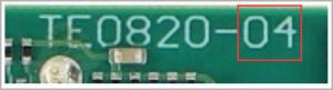
| 2020-08-14 | 04 | - Fixed DDR4 connection (BG1), support B-die DDR4 Industrial grade chips
- Added R93, changed value C62, change obsolete U28
- Added R89 (10R)
- Added additional caps 4.7uF to PS_AVTT/PS_AVCC (Xilinx doc UG583)
- Changed R51 20k ->10K (PS_AVCC = 0.85V, Xilinx doc DS925 v1.17)
- Fixed DDR4 connection (Alert)
- Added 3.3V signal to CPLD
- Added testpoints
- LIB components update
| PCN-20200616 | TE0820-4 | | 2019-01-02 | 03 | - Fixed VCU connection: add additional DCDC (0.9V)
- LIB components update
- Change package 1K resistors (0402 -> 0201)
- Added LEDs (1x user LED, 1x LED for ERR_STATUS, 1xLED for ERR_OUT)
- Change obsolete 2xSPI Flash (256MBit) -> 2xSPI Flash (512MBit)
- Added additional DCDCs (PL_VCCINT_IO, PS_FP0V85)
- Changed DCDC (U5) 6A (optional 4A)
| PCN-20190110 | TE0820-03 | | 2017-08-17 | 02 | - Added MAC EEPROM (slave address)
- LIB components update
- Fixed SD Card connection
- Fixed sense connection from DCDC
- Made correct power connection for VCU (removed DCDC, added resistors and caps like as Xilinx recommended)
- Added resistors for variants (ZU+ with/without VCU)
- Added termination resistors (240R) to VRP pins fro all HP-banks
| PCN-20171117 | TE0820-02 | | 2016-12-23 | 01 | Prototype only | - | TE0820-01 |
|
| Scroll Title |
|---|
| anchor | Figure_6 |
|---|
| title-alignment | center |
|---|
| title | Figure 6: Module hardware revision number |
|---|
|
| Scroll Ignore |
|---|
| scroll-pdf | true |
|---|
| scroll-office | true |
|---|
| scroll-chm | true |
|---|
| scroll-docbook | true |
|---|
| scroll-eclipsehelp | true |
|---|
| scroll-epub | true |
|---|
| scroll-html | true |
|---|
| | draw.io Diagram |
|---|
| border | true |
|---|
| |
|---|
| diagramName | TE0820_HV_HRH HRH |
|---|
| simpleViewer | false |
|---|
| width | |
|---|
| links | auto |
|---|
| tbstyle | top |
|---|
| lbox | true |
|---|
| diagramWidth | 205 |
|---|
| revision | 1 |
|---|
|
|
| Scroll Only |
|---|
| scroll-pdf | true |
|---|
| scroll-office | true |
|---|
| scroll-chm | true |
|---|
| scroll-docbook | true |
|---|
| scroll-eclipsehelp | true |
|---|
| scroll-epub | true |
|---|
| scroll-html | true |
|---|
| 
|
|
Document Change History
| Page properties |
|---|
|
- Note this list must be only updated, if the document is online on public doc!
- It's semi automatically, so do following
Add new row below first Copy "Page Information Macro (date)" Macro-Preview, Metadata Version number, Author Name and description to the empty row. Important Revision number must be the same as the Wiki document revision number Update Metadata = "Page Information Macro (current-version)" Preview+1 and add Author and change description. --> this point is will be deleted on newer pdf export template - Metadata is only used of compatibility of older exports
|
| Scroll Title |
|---|
| anchor | Table_RH_DCH |
|---|
| title-alignment | center |
|---|
| title | Document change history. |
|---|
|
| Scroll Table Layout |
|---|
| orientation | portrait |
|---|
| sortDirection | ASC |
|---|
| repeatTableHeaders | default |
|---|
| style | |
|---|
| widths | |
|---|
| sortByColumn | 1 |
|---|
| sortEnabled | false |
|---|
| cellHighlighting | true |
|---|
|
| Date | Revision | Contributor | Description |
|---|
| Page info |
|---|
| infoType | Modified date |
|---|
| dateFormat | yyyy-MM-dd |
|---|
| type | Flat |
|---|
|
| | Page info |
|---|
| infoType | Current version |
|---|
| prefix | v. |
|---|
| type | Flat |
|---|
| showVersions | false |
|---|
|
| | Page info |
|---|
| infoType | Modified by |
|---|
| type | Flat |
|---|
| showVersions | false |
|---|
|
| | | 2020-09-18 | v.95 | Pedram Babakhani | - Update to REV04
- Update the TRM format
- Technical Information update
| | 2020-03-16 | v.87 | John Hartfiel | - Corrected PLL section
- Corrected Designators USB, ETH PHY, CLK section
| | 2020-02-03 | v.85 | Martin Rohrmüller | - Corrected #MIOs for QSPI and USB in block diagram
| | 2019-11-28 | v.81 | Martin Rohrmüller | - typo and designator in section USB interface corrected
| | 2019-10-30 | v.80 | John Hartfiel | | | 2019-09-17 | v79 | Martin Rohrmüller | - Updated according to PCN-20190110: eMMC, QSPI-Flash
| | v.78 | Martin Rohrmüller | - Corrected PJTAG Mio Pin29 in table 8
| 2019-05-08 | v.77 | John Hartfiel | - Corrected EEPROM I2C Address
- Correction USB PHY connection
| | v.74 | John Hartfiel | | | v.73 | John Hartfiel | - typo correction
- update CPLD section
- add LEDs to component list
- add 3D picture of REV03 instead of REV01 picture
| | v.69 | Ali Naseri | | | v.61 | John Hartfiel | - Rework chapter currently available products
- add PJTAG note to MIOtable
| | 2018-03-12 | v.54 |
| - Correction Power Rail Section
| | 2017-11-20 | v.51 | John Hartfiel | - Correction Default MIO Configuration Table
| | 2017-11-10 | v.50 | John Hartfiel | - Replace B2B connector section
| | 2017-10-18 | v.49 | John Hartfiel | | | 2017-09-25 | v.48 | John Hartfiel | - Correction in the "Board to Board (B2B) I/Os" section
- Update in the "Variants Currently In Production" section
| | 2017-09-18 | v.47 | John Hartfiel | | | 2017-08-30 | v.46 | Jan Kumann | | | | John Hartfiel | - Correction in the "Key Features" section.
| | 2017-08-21 | v.34 | John Hartfiel | - "Initial delivery state" section updated.
| | 2017-08-21 | v.33 | Jan Kumann | - HW revision 02 block diagram added.
- Power distribution and power-on sequence diagram added.
- System Controller CPLD and DDR4 SDRAM sections added.
- TRM update to the template revision 1.6
- Weight section removed.
- Few minor corrections.
| | | John Hartfiel | - Style changes
- Updated "Boot Mode", "HW Revision History", "Variants Currently In Production" sections
- Correction of MIO SD Pin-out, System Controller chapter
- Update and new sub-sections on "On Board Peripherals and Interfaces" sections
| 2017-08-07 | v.5 | Jan Kumann | | -- | all | | Page info |
|---|
| infoType | Modified users |
|---|
| type | Flat |
|---|
| showVersions | false |
|---|
|
| |
|
Table 21: Document change history
Disclaimer
| Include Page |
|---|
| IN:Legal Notices |
|---|
| IN:Legal Notices |
|---|
|