or subsection by assigning advance link using: #NameOfTheSection Example: | Chip/Interface | Designator | Connected To | Notes |
|---|
| ETH PHY | U10 | | Gigabit ETH PHY |
|
| Scroll Title |
|---|
| anchor | Table_OBP |
|---|
| title | On board peripherals |
|---|
|
| Scroll Table Layout |
|---|
| orientation | portrait |
|---|
| sortDirection | ASC |
|---|
| repeatTableHeaders | default |
|---|
| style | |
|---|
| widths | |
|---|
| sortByColumn | 1 |
|---|
| sortEnabled | false |
|---|
| cellHighlighting | true |
|---|
|
|
System Controller Intel MAX 10
The TEI0022 is equipped with an Intel MAX 10 (U41) which is the central system management unit where essential control signals are logically linked by the implemented logic of the FPGA firmware. This generates output signals to control the system, the on-board peripherals and the interfaces. Interfaces like JTAG are by-passed, forwarded and controlled by the System Controller. Other tasks of the System Controller are the monitoring of the power-on sequence and configuration of the Intel Cyclone V FPGA. The functionalities and configuration of the pins depend on its firmware.
Intel Cyclone V
The Intel Cyclone V device used at the TEI0022 board is a SoC with integrated ARM-based HPS. The 5CSEMA5F31C8N version delivers one hard memory controller, 80K logic elements in an FineLineBGA (FBGA) with 896 pins for the commercial temperature range of TJ = 0...85 °C with speed grade eight.
DDR3 SDRAM
| Page properties |
|---|
|
Notes : Minimum and Maximum density of DDR3 SDRAM must be mentioned for other assembly options. (pay attention to supported address length for DDR3) |
The TEI0022 SoM has one GByte volatile DDR3 SDRAM memory per FPGA (U26, U27) and HPS (U28, U29) for storing user application code and data.
- Part number: IS43TR16256BL-125KBLI
- Supply voltage: 1.5 V
- Speed: TBD
- Temperature: TC = -40 °C up to 95 °C
Gigabit Ethernet PHY
On-board Gigabit Ethernet PHY (U1) is provided with Analog Devices ADIN1300. The Ethernet PHY RGMII interface is connected to the Intel Cyclone V HPS. I/O voltage is fixed at 3.3 V. The reference clock input of the PHY is supplied from the on-board 25.0 MHz oscillator (U48).
| Scroll Title |
|---|
| anchor | Table_OBP_ETH |
|---|
| title | Ethernet PHY to HPS connections |
|---|
|
| Scroll Table Layout |
|---|
| orientation | portrait |
|---|
| sortDirection | ASC |
|---|
| repeatTableHeaders | default |
|---|
| style | |
|---|
| widths | |
|---|
| sortByColumn | 1 |
|---|
| sortEnabled | false |
|---|
| cellHighlighting | true |
|---|
|
| Bank | Signal Name | Signal Description |
|---|
| 7B | ETH_TXCK | RGMII Transmit Reference Clock | | 7B | ETH_TXD0 | RGMII Transmit Data 0 | | 7B | ETH_TXD1 | RGMII Transmit Data 1 | | 7B | ETH_TXD2 | RGMII Transmit Data 2 | | 7B | ETH_TXD3 | RGMII Transmit Data 3 | | 7B | ETH_TXCTL | RGMII Transmit Control | | 7B | ETH_RXCK | RGMII Receive Reference Clock | | 7B | ETH_RXD0 | RGMII Receive Data 0 | | 7B | ETH_RXD1 | RGMII Receive Data 1 | | 7B | ETH_RXD2 | RGMII Receive Data 2 | | 7B | ETH_RXD3 | RGMII Receive Data 3 | | 7B | ETH_RXCTL | RGMII Receive Control | | 7C | ETH_RST | Reset | | 7B | ETH_MDC | Management Data Clock | | 7B | ETH_MDIO | Management Data I/O | | 7B | PHY_INT | Interrupt |
|
High-Speed USB ULPI PHY
USB PHY (U8) is provided by USB3320C from Microchip. The ULPI interface is connected to the Intel Cyclone V HPS. I/O voltage is fixed at 3.3 V and PHY reference clock input is supplied from the on-board 24.0 MHz oscillator (U34).
| Scroll Title |
|---|
| anchor | Table_OBP_USB_PHY |
|---|
| title | USB PHY interface connections |
|---|
|
| Scroll Table Layout |
|---|
| orientation | portrait |
|---|
| sortDirection | ASC |
|---|
| repeatTableHeaders | default |
|---|
| style | |
|---|
| widths | |
|---|
| sortByColumn | 1 |
|---|
| sortEnabled | false |
|---|
| cellHighlighting | true |
|---|
|
| PHY Pin | Connected to | Notes |
|---|
| ULPI | Intel Cyclone V HPS (U10) |
| | REFCLK | 24 MHz from on board oscillator (U34) |
| | REFSEL[0..2] | High (3.3 V) |
| | RESETB | Intel Cyclone V HPS (U10) and Intel MAX 10 (U41) |
| | DP, DM | 4-port USB 2.0 Hub (U33) |
| | CPEN | Not Connected. |
| | VBUS | Pull-up to 5 V. |
| | ID | Not Connected. |
|
|
4-Port USB 2.0 Hub
On the TEI0022 board there are up to four USB 2.0 Hi-Speed ports available (J2, J12). The USB 2.0 ports are provided by Microchip Cypress USB2514B 4-port USB 2.0 Hub controller (U33) which is connected to the USB PHY USB3320C (U8) connected to the Intel Cyclone V HPS via ULPI.
HDMI Transmitter
The TEI0022 board provides an HDMI interface routed to the Intel Cyclone FPGA (U10). The HDMI interface is created by the HDMI transmitter ADV7511 provided by Analog Devices. The HDMI transmitter is incorporated in conjunction with the HDMI protection circuit TI TPD12S016 for more signal robustness.
| Scroll Title |
|---|
| anchor | Table_OBP_HDMI |
|---|
| title | HDMI connector signals and pins |
|---|
|
| Scroll Table Layout |
|---|
| orientation | portrait |
|---|
| sortDirection | ASC |
|---|
| repeatTableHeaders | default |
|---|
| style | |
|---|
| widths | |
|---|
| sortByColumn | 1 |
|---|
| sortEnabled | false |
|---|
| cellHighlighting | true |
|---|
|
| HDMI connector J11 | Signal Schematic Name | Connected to | Notes |
|---|
| Pin 1, 3 | HDMI_TX2_P / HDMI_TX2_N | HDMI transmitter, Pin 43, 42 | also connected to HDMI protection circuit | | Pin 4, 6 | HDMI_TX1_P / HDMI_TX1_N | HDMI transmitter, Pin 40, 39 | also connected to HDMI protection circuit | | Pin 7, 9 | HDMI_TX0_P / HDMI_TX0_N | HDMI transmitter, Pin 36, 35 | also connected to HDMI protection circuit | | Pin 10, 12 | HDMI_TXC_P / HDMI_TXC_N | HDMI transmitter, Pin 33, 32 | also connected to HDMI protection circuit | | Pin 13 | CEC_B | HDMI transmitter, Pin 48 | HDMI CEC, wired through HDMI protection circuit | | Pin 15 | SCL_B | HDMI transmitter, Pin 53 | HDMI I²C clock line, wired through HDMI protection circuit | | Pin 16 | SDA_B | HDMI transmitter, Pin 54 | HDMI I²C data line, wired through HDMI protection circuit | | Pin 19 | HPD_B | HDMI transmitter, Pin 30 | Hot Plug Detect, wired through HDMI protection circuit | | Pin 18 | 5V_HDMI | HDMI protection circuit, Pin 13 | 5V supply voltage, wired through HDMI protection circuit |
|
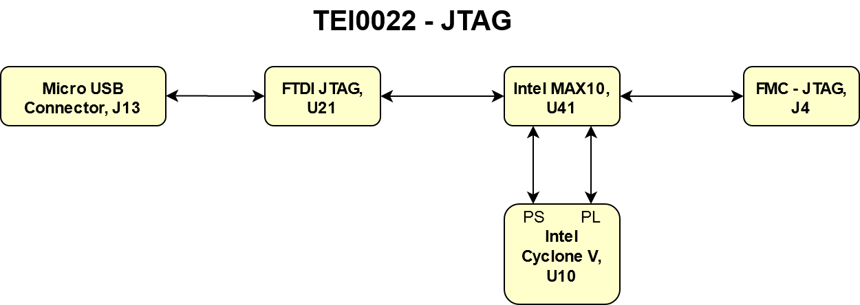
FTDI (JTAG)
Please refer to the section "Micro USB Connector (JTAG)".
FTDI (UART)
Please refer to the section "Micro USB Connector (UART)".
DIP-Switches
There are three 4-bit DIP-switches present on the TEI0022 board to configure options and set parameters. The following section describes the functionalities of the particular switches.
DIP-Switch S2
The table below describes the functionalities of the switches of DIP-switch S2 at their single positions:
| Scroll Title |
|---|
| anchor | Table_OBP_DIP_S2 |
|---|
| title | DIP-switch S2 functionality description |
|---|
|
| Scroll Table Layout |
|---|
| orientation | portrait |
|---|
| sortDirection | ASC |
|---|
| repeatTableHeaders | default |
|---|
| style | |
|---|
| widths | |
|---|
| sortByColumn | 1 |
|---|
| sortEnabled | false |
|---|
| cellHighlighting | true |
|---|
|
| DIP-switch S2 | Position ON | Position OFF | Notes |
|---|
| S4-1 | HPS_SW1 is low | HPS_SW1 is high | User switch | | S4-2 | HPS_SW2 is low | HPS_SW2 is high | User switch | | S4-3 | FPGA_SW1 is low | FPGA_SW1 is high | User switch | | S4-4 | FPGA_SW2 is low | FPGA_SW2 is high | User switch |
|
DIP-Switch S7
The table below describes the functionalities of the switches of DIP-switch S7 at their single positions:
| Scroll Title |
|---|
| anchor | Table_OBP_DIP_S7 |
|---|
| title | DIP-switch S7 functionality description |
|---|
|
| Scroll Table Layout |
|---|
| orientation | portrait |
|---|
| sortDirection | ASC |
|---|
| repeatTableHeaders | default |
|---|
| style | |
|---|
| widths | |
|---|
| sortByColumn | 1 |
|---|
| sortEnabled | false |
|---|
| cellHighlighting | true |
|---|
|
| DIP-switch S7 | Position ON | Position OFF | Notes |
|---|
| S7-1 | HPS_SPI_SS/BOOTSEL0 is low | HPS_SPI_SS/BOOTSEL0 is high | Boot select (Firmware dependent) | | S7-2 | QSPI_CS/BOOTSEL1 is low | QSPI_CS/BOOTSEL1 is high | Boot select (Firmware dependent) | | S7-3 | JTAGSEL0 is low | JTAGSEL0 is high | JTAG select (Firmware dependent) | | S7-4 | JTAGSEL1 is low | JTAGSEL1 is high | JTAG select (Firmware dependent) |
|
DIP-Switch S8
The table below describes the functionalities of the switches of DIP-switch S8 at their single positions:
| Scroll Title |
|---|
| anchor | Table_OBP_DIP_S8 |
|---|
| title | DIP-switch S8 functionality description |
|---|
|
| Scroll Table Layout |
|---|
| orientation | portrait |
|---|
| sortDirection | ASC |
|---|
| repeatTableHeaders | default |
|---|
| style | |
|---|
| widths | |
|---|
| sortByColumn | 1 |
|---|
| sortEnabled | false |
|---|
| cellHighlighting | true |
|---|
|
| DIP-switch S8 | Position ON | Position OFF | Notes |
|---|
| S8-1 | VID0_SW is low | VID0_SW is high | FMC_VADJ selection (Firmware dependent) | | S8-2 | VID1_SW is low | VID1_SW is high | FMC_VADJ selection (Firmware dependent) | | S8-3 | VID2_SW is low | VID2_SW is high | FMC_VADJ selection (Firmware dependent) | | S8-4 | JTAGEN is high | JTAGEN is low | JTAG select |
|
There are four buttons present on the TEI0022 board. The following section describes the functionalities of the particular buttons. The final functionality is set by the management Intel MAX10.
| Scroll Title |
|---|
| anchor | Table_OBP_DIP_Buttons |
|---|
| title | Buttons functionality description |
|---|
|
| Scroll Table Layout |
|---|
| orientation | portrait |
|---|
| sortDirection | ASC |
|---|
| repeatTableHeaders | default |
|---|
| style | |
|---|
| widths | |
|---|
| sortByColumn | 1 |
|---|
| sortEnabled | false |
|---|
| cellHighlighting | true |
|---|
|
| Button | Position ON | Position OFF | Notes |
|---|
| S1 | HPS_RST#_SW is low | HPS_RST#_SW is high | Reset (cold) the Intel Cyclone V HPS (Firmware dependent) | | S3 | HPS_WARM_RST#_SW is low | HPS_WARM_RST#_SW is high | Reset (warm) the Intel Cyclone V HPS (Firmware dependent) | | S4 | FPGA_RST#_SW is low | FPGA_RST#_SW is high | Reset the Intel Cyclone V FPGA (Firmware dependent) | | S5 | USER_BTN_SW is low | USER_BTN_SW is high | User button (Firmware dependent) |
|
On-Board LEDs
The TEI0022 board is equipped with several LEDs to signal current states and activities. The functionality of the LEDs D11...14 are user LEDs. The LED D8 shows the Intel Cyclone V configuration progress. LEDs D15, D18...19 shows the UART connection and the other LEDs mentioned in the table are supply power status LEDs.
| Scroll Title |
|---|
| anchor | Table_OBP_LED |
|---|
| title | On-board LEDs |
|---|
|
| Scroll Table Layout |
|---|
| orientation | portrait |
|---|
| sortDirection | ASC |
|---|
| repeatTableHeaders | default |
|---|
| style | |
|---|
| widths | |
|---|
| sortByColumn | 1 |
|---|
| sortEnabled | false |
|---|
| cellHighlighting | true |
|---|
|
| Designator | Color | Connected to | Active Level | Note |
|---|
| D11 | Green | Intel Cyclone V HPS | H | User LED | | D12 | Green | Intel Cyclone V HPS | H | User LED | | D13 | Green | Intel Cyclone V FPGA | H | User LED | | D14 | Green | Intel Cyclone V FPGA | H | User LED | | D8 | Green | Intel Cyclone V FPGA, Intel MAX 10 | L | Status: Configuration "Done" | | D15 | Green | FT234XD | L | UART | | D18 | Green | UART TX | L | UART | | D19 | Green | UART RX | L | UART | | D21 | Green | +12.0V | H | Status of +12.0V voltage rail | | D1 | Green | +12.0V_FMC | H | Status of +12.0V_FMC voltage rail | | D2 | Green | +5.0V | H | Status of +5.0V voltage rail | | D3 | Green | +3.3V | H | Status of +3.3V voltage rail | | D20 | Green | +3.3V_MAX10 | H | Status of +3.3V_MAX10 voltage rail | | D22 | Green | +3.3V_FMC | H | Status of +3.3V_FMC voltage rail | | D4 | Green | +2.5V | H | Status of +2.5V voltage rail | | D5 | Green | Intel MAX 10 | H | Status of +1.8V voltage rail | | D7 | Green | Intel MAX 10 | H | Status of VCC voltage rail | | D9 | Green | Intel MAX 10 | H | Status of FMC_VADJ voltage rail | | D6 | Green | Intel MAX 10 | H | Status of VDD_DDR_FPGA voltage rail | | D23 | Green | Intel MAX 10 | H | Status of VDD_DDR_HPS voltage rail | | D17 | Green | Intel MAX 10 | H | Status of VTT_DDR_FPGA voltage rail | | D10 | Green | Intel MAX 10 | H | Status of VTT_DDR_HPS voltage rail | | D25 | Red | Intel MAX 10 | H | Status |
|
Temperature Sensor
The temperature sensor ADT7410 (U16) is implemented on the TEI0022 board.
Quad SPI Flash Memory
| Page properties |
|---|
|
Notes : Minimum and Maximum density of quad SPI flash must be mentioned for other assembly options. |
Two 256 Mbit (32 MByte) Quad SPI Flash Memory (Micron MT25QL256ABA8E12, U6, U15) are provided for FPGA and HPS configuration file storage. After configuration process completes the remaining free memory can be used for application data storage. All four SPI data lines are connected to the FPGA or the HPS allowing x1, x2 or x4 data bus widths to be used. The maximum data transfer rate depends on the bus width and clock frequency.
Quad SPI Flash memory U6 is connected to the HPS bank 7B and U15 to FPGA bank 3A.
| Scroll Title |
|---|
| anchor | Table_OBP_QSPI_HPS |
|---|
| title | HPS Quad SPI interface signals and connections |
|---|
|
| Scroll Table Layout |
|---|
| orientation | portrait |
|---|
| sortDirection | ASC |
|---|
| repeatTableHeaders | default |
|---|
| style | |
|---|
| widths | |
|---|
| sortByColumn | 1 |
|---|
| sortEnabled | false |
|---|
| cellHighlighting | true |
|---|
|
| Signal Name | QSPI Flash Memory U6 Pin | FPGA Pin |
|---|
| QSPI_CS/BOOTSEL1 | S#, Pin C2 | Bank 7B, Pin A18 | | QSPI_CLK | C, Pin B2 | Bank 7B, Pin D19 | | QSPI_DATA0 | DQ0, Pin D3 | Bank 7B, Pin C20 | | QSPI_DATA1 | DQ1, Pin D2 | Bank 7B, Pin H18 | | QSPI_DATA2 | DQ2, Pin C4 | Bank 7B, Pin A19 | | QSPI_DATA3 | DQ3, Pin D4 | Bank 7B, Pin E19 |
|
| Scroll Title |
|---|
| anchor | Table_OBP_QSPI_FPGA |
|---|
| title | FPGA Quad SPI interface signals and connections |
|---|
|
| Scroll Table Layout |
|---|
| orientation | portrait |
|---|
| sortDirection | ASC |
|---|
| repeatTableHeaders | default |
|---|
| style | |
|---|
| widths | |
|---|
| sortByColumn | 1 |
|---|
| sortEnabled | false |
|---|
| cellHighlighting | true |
|---|
|
| Signal Name | QSPI Flash Memory U15 Pin | FPGA Pin |
|---|
| nCSO | S#, Pin C2 | Bank 3A, Pin AB8 | | AS_DCK | C, Pin B2 | Bank 3A, Pin U7 | | AS_DATA0 | DQ0, Pin D3 | Bank 3A, Pin AE6 | | AS_DATA1 | DQ1, Pin D2 | Bank 3A, Pin AE5 | | AS_DATA2 | DQ2, Pin C4 | Bank 3A, Pin AE8 | | AS_DATA3 | DQ3, Pin D4 | Bank 3A, Pin AC7 |
|
EEPROM
The TEI0022 board contains two EEPROMs for configuration and general user purposes.
| Scroll Title |
|---|
| anchor | Table_OBP_EEPROM |
|---|
| title | On-board configuration EEPROMs overview |
|---|
|
| Scroll Table Layout |
|---|
| orientation | portrait |
|---|
| sortDirection | ASC |
|---|
| repeatTableHeaders | default |
|---|
| style | |
|---|
| widths | |
|---|
| sortByColumn | 1 |
|---|
| sortEnabled | false |
|---|
| cellHighlighting | true |
|---|
|
| EEPROM Model | I2C Address | Designator | Memory Density | Purpose | Notes |
|---|
| 24AA025E48T-I/OT | 0x50 | U38 | 2 KBit | Ethernet MAC |
| | 93AA56BT-I/OT | - | U31 | 2 KBit | JTAG Configuration |
|