Page History
| Scroll Ignore |
|---|
Download PDF Version of this Document.
|
| Scroll pdf ignore | ||||
|---|---|---|---|---|
Table of Contents
|
...
All this on a tiny footprint, smaller than half a credit card, at the most competitive price.
Block diagram
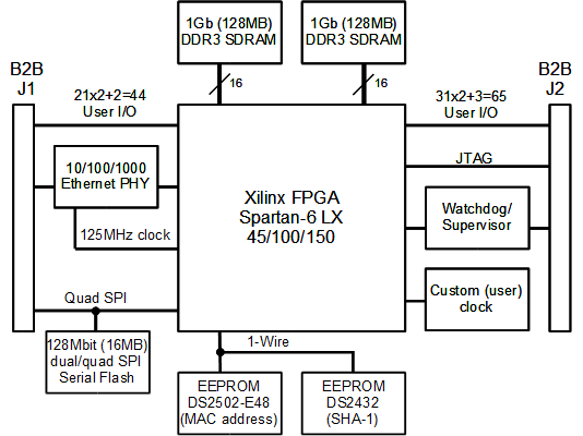
Block diagram of the GigaBee XC6SLX board
Main components
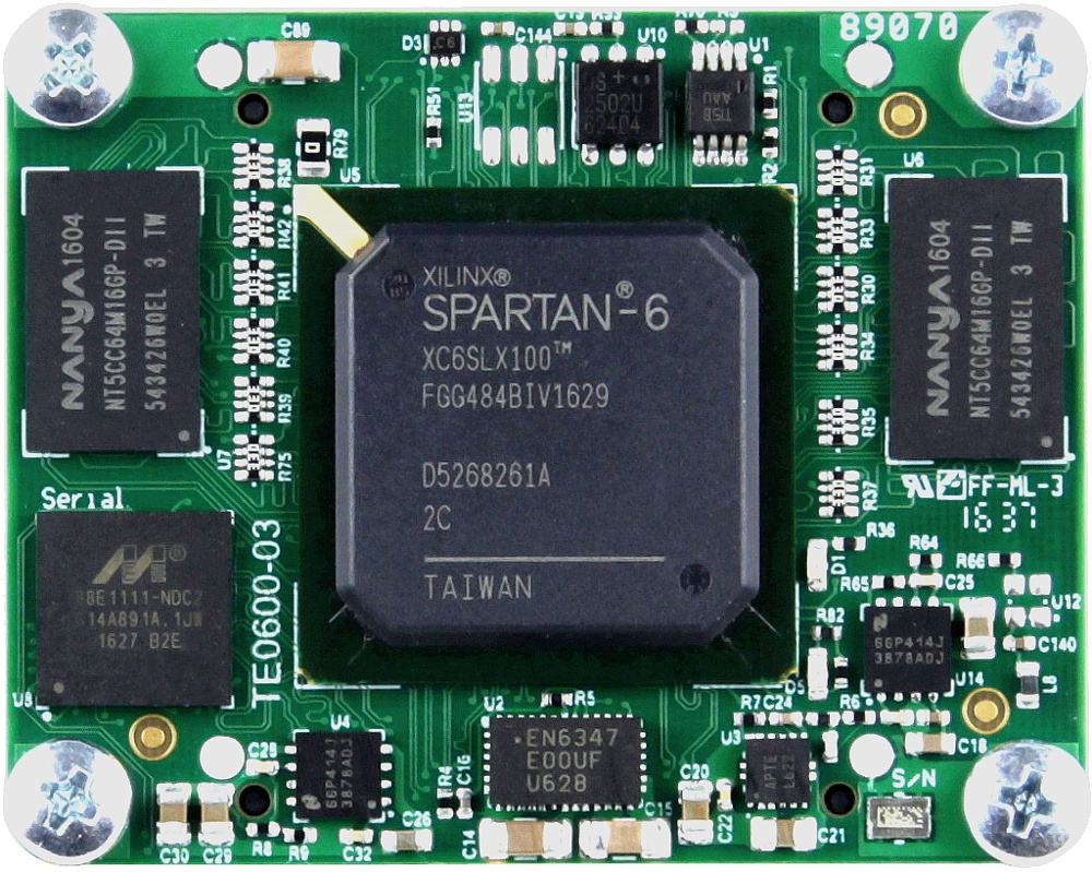
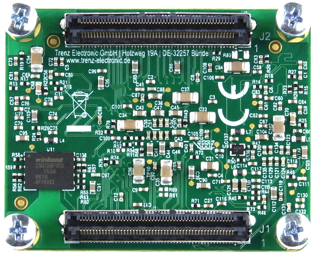
Pictures were photographed from revision 3 and serve for informational purposes only.
Top side:
- Xilinx Spartan-6 LX FPGA
- clock generator
- 10/100/1000 Mbps Ethernet PHY
- protected 1-Wire EEPROM
- DDR3-SDRAM
- DC-DC converters
...
Industrial-grade Xilinx Spartan-6 LX FPGA micromodule (LX45 / LX100 / LX150)
10/100/1000 tri-speed Gigabit Ethernet transceiver (PHY)
2 x 16-bit-wide 1 Gb (128 MB) or 4 Gb (512 MB) DDR3 SDRAM
128 Mb (16 MB) SPI Flash memory (for configuration and operation) accessible through:
1 kb protected 1-Wire EEPROM with SHA-1 Engine
JTAG port (SPI indirect)
FPGA configuration through:
B2B connector
JTAG port
SPI Flash memory
Plug-on module with 2 × 100-pin high-speed hermaphroditic strips
Up to 52 differential, up to 109 single-ended (+ 1 dual-purpose) FPGA I/O pins available on B2B strips
46.0 A 0 A x 1.2 V 2 V power rail
3.0 A x 1.5 A x 1.5 V 5 V power rail
- 2x 1A x 2.5V power rail
125 MHz reference clock signal
Single-ended custom oscillator (option)
eFUSE bit-stream encryption (LX100 or larger)
1 user LED
Evenly-spread supply pins for good signal integrity
...
Boards – GigaBee XC6SLX 45/100/150
Base board – TE0603-02
Power supply – 5 V from 5 V for baseboard
Connected Gigabit Ethernet cable
...
Board power supply diagram
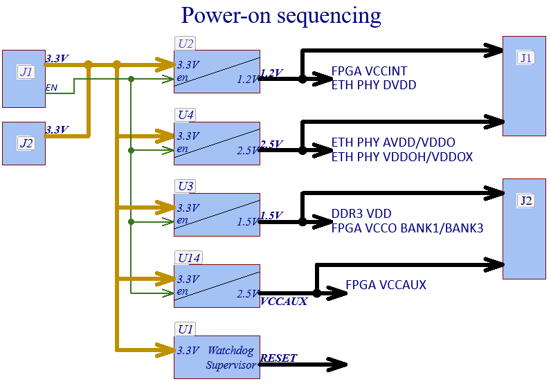
Power Supply Sources
...
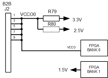
FPGA VCCIO power options are shown below. Default values for configurable voltages are shown in braces.
| Bank | Supply voltage |
|---|---|
| B0 | VCCIO 0 VCCIO0 (3. 3 V3V) |
| B1 | VCCIO 1 VCCIO1 (1.5 V5V) |
| B2 | VCCIO2 (3.3 V3V) |
| B3 | VCCIO3 (1.5 V5V) |
Bank 0 power supply VCCIO 0 VCCIO0 can be configured by user to 3.3 V3 V, 2.5 V 5 V or 1.5 V5 V, see Chapter VCCIO0 Power Rail. Bank Banks 1 and 3 VCCIO supply voltage is configured to 1.5 V 5 V to communicate with DDR3 SDRAM memory chip.
...
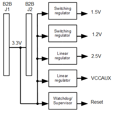
| 3.3V Power Rail | It is the main internal power rail and must be supplied from an external power source. It supplies the other following power rails:
|
|---|---|
| 1.2V Power Rail | It is converted from the 3.3V rail by a switching voltage regulator and can provide up to 4.0 A 6A to:
|
| 1.5V Power Rail | It is converted from the 3.3V rail by a switching voltage regulator and can provide up to 1.5 A 3A to:
|
| 2.5V Power Rail | It is converted from the 3.3V rail by a linear voltage regulator and can provide up to 0.8 A 1A to:
|
| VCCAUX Power Rail | It is converted from the 3.3V rail by a linear voltage regulator and can provide up to 0.8 A 1A to:
|
| VCCIO0 Power Rail | There are 4 options to supply this rail:
It supplies:
Figure below show simplified schematic of power options. Dashed resistors are not populated by default.
|
...
power-rail | nominal | maximum | power | system | user |
|---|---|---|---|---|---|
| 3.3V | 3.3 | 2.4 | J1, J2 | module | J1 (≤1.2 A) |
| 2.5V | 2.5 | 1.0.8 | 3.3V ? linear | Ethernet | J1 (≤0.3 A) |
| 1.5V | 1.51 | 3.50 | 3.3V ? switch | DDR3 SDRAM | J1 (≤0.3 A) |
| 1.2V | 1.2 | 46.0 | 3.3V ? switch | VCCINT | J1 (≤0.6 A) |
| VCCAUX | 2.5 | 1.0.8 | 3.3V ? linear | FPGA | J2 (≤0.3 A) |
| VCCCIO0 | 1.2, 1.5, 1.8, 2.5, 3.3 | 0.9 | J2 or 2.5V or 3.3V | VCCO (0) | J2 (≤0.9 A) |
Power Supervision
...
For more information see Winbond W25Q128FV W25Q128JVEIQ (W25Q128BV till REV 02or W25Q128FV in old revisions) product overview.
Flash can be programmed in several ways:
...
| Note | ||
|---|---|---|
| ||
Note: For correct generation start, PHY should receive reset pulse. Recommended way to do it it's to connect PHY reset signal (ETHERNET_PHY_RST_N) to LOCKED output of corresponding DCM (DCM which use 125 MHz from PHY). |
The module also provides the footprint for custom additional 3.3 V 3 V single-ended oscillator (U12) which can be installed as an option used as a system and user clock for the FPGA (FPGA input pin Y13).
User LED
...
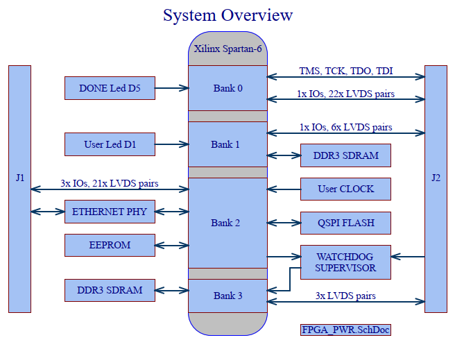
| FPGA Bank | Single-ended | Differential | Total | VCCIO |
| Bank 0 | 1 | 22 | 45 | VCCIO 0 VCCIO0 (3.3 V3V) |
| Bank 1 | 1 | 6 | 13 | VCCIO 1 VCCIO1 (1.5 V5V) |
| Bank 2 | 3 | 21 | 45 | VCCIO2 (3.3 V3V) |
| Bank 3 | 0 | 3 | 6 | VCCIO3 (1.5 V5V) |
| 5 | 52 | 109 |
B2B signals count
Pin Labeling
...
| J1 pin | Net | Type | FPGA pin | Net Length | J1 pin | Net | Type | FPGA pin | Net Length |
| 1 | 3.3V | POW | - | - | 2 | GND | GND | - | - |
| 3 | 3.3V | POW | - | - | 4 | PHY_MDI0_P | PHY | - | - |
| 5 | 3.3V | POW | - | - | 6 | PHY_MDI0_N | PHY | - | - |
| 7 | 3.3V | POW | - | - | 8 | GND | GND | - | - |
| 9 | 3.3V | POW | - | - | 10 | PHY_MDI1_P | PHY | - | - |
| 11 | 3.3V | POW | - | - | 12 | PHY_MDI1_N | PHY | - | - |
| 13 | 3.3V | POW | - | - | 14 | PHY_AVDD | PHY | - | - |
| 15 | 3.3V | POW | - | - | 16 | PHY_MDI2_P | PHY | - | - |
| 17 | PHY_L10 | PHY | - | - | 18 | PHY_MDI2_N | PHY | - | - |
| 19 | PHY_L100 | PHY | - | - | 20 | GND | GND | - | - |
| 21 | PHY_L1000 | PHY | - | - | 22 | PHY_MDI3_P | PHY | - | - |
| 23 | PHY_DUP | PHY | - | - | 24 | PHY_MDI3_N | PHY | - | - |
| 25 | PHY_LED_TX | PHY | - | - | 26 | GND | GND | - | - |
| 27 | PHY_LED_RX | PHY | - | - | 28 | EN | TE | - | - |
| 29 | GND | GND | - | - | 30 | INIT | CONFIG | T6 | - |
| 31 | B2B_B2_L57_N | DIO | AB4 | 812.66mm3056mm | 32 | B2B_B2_L32_N | SIO | AB11 | 89.12mm2307mm |
| 33 | B2B_B2_L57_P | DIO | AA4 | 912.84mm3446mm | 34 | GND | GND | - | - |
| 35 | B2B_B2_L49_N | DIO | AB6 | 810.66mm9076mm | 36 | B2B_B2_L60_P | DIO | T7 | 912.96mm8674mm |
| 37 | B2B_B2_L49_P | DIO | AA6 | 911.58mm4038mm | 38 | B2B_B2_L60_N | DIO | R7 | 1113.16mm3583mm |
| 39 | 2.5V | POW | - | - | 40 | B2B_B2_L59_N | DIO | R8 | 1113.42mm4941mm |
| 41 | 1.2V | POW | - | - | 42 | B2B_B2_L59_P | DIO | R9 | 1113.36mm4584mm |
| 43 | 1.2V | POW | - | - | 44 | GND | GND | - | - |
| 45 | B2B_B2_L48_N | DIO | AB7 | 914.98mm447mm | 46 | B2B_B2_L44_N | DIO | Y10 | 1113.34mm4331mm |
| 47 | B2B_B2_L48_P | DIO | Y7 | 1014.98mm6069mm | 48 | B2B_B2_L44_P | DIO | W10 | 1013.21mm0478mm |
| 49 | B2B_B2_L45_N | DIO | AB8 | 1011.60mm3986mm | 50 | B2B_B2_L42_N | DIO | W11 | 79.52mm889mm |
| 51 | B2B_B2_L45_P | DIO | AA8 | 11.053mm642mm | 52 | B2B_B2_L42_P | DIO | V11 | 810.36mm2701mm |
| 53 | GND | GND | - | - | 54 | GND | GND | - | - |
| 55 | B2B_B2_L43_N | DIO | AB9 | 13.75mm1392mm | 56 | B2B_B2_L18_P | DIO | V13 | 710.94mm5384mm |
| 57 | B2B_B2_L43_P | DIO | Y9 | 1213.97mm5123mm | 58 | B2B_B2_L18_N | DIO | W13 | 610.96mm0455mm |
| 59 | B2B_B2_L41_N | DIO | AB10, AB13 | 1015.33mm7999mm | 60 | B2B_B2_L8_N | DIO | U16 | 912.92mm2993mm |
| 61 | B2B_B2_L41_P | DIO | AA10, Y13 | 1116.01mm1771mm | 62 | B2B_B2_L8_P | DIO | U17 | 912.94mm2993mm |
| 63 | GND | GND | - | - | 64 | GND | GND | - | - |
| 65 | B2B_B2_L21_P | DIO | Y15 | 1314.12mm8399mm | 66 | B2B_B2_L11_P | DIO | V17 | 810.31mm5343mm |
| 67 | B2B_B2_L21_N | DIO | AB15 | 1214.37mm6254mm | 68 | B2B_B2_L11_N | DIO | W17 | 710.29mm1532mm |
| 69 | B2B_B2_L15_P | DIO | Y17 | 1413.20mm2958mm | 70 | B2B_B2_L6_P | DIO | W18 | 79.40mm5851mm |
| 71 | B2B_B2_L15_N | DIO | AB17 | 13.77mm1454mm | 72 | B2B_B2_L6_N | DIO | Y18 | 69.94mm1811mm |
| 73 | GND | GND | - | - | 74 | GND | GND | - | - |
| 75 | B2B_B2_L31_N | SIO | AB12 | 1214.30mm3436mm | 76 | B2B_B2_L5_P | DIO | Y19 | 68.18mm398mm |
| 77 | SUSPEND | SYS | N15 | 1921.23mm1709mm | 78 | B2B_B2_L5_N | DIO | AB19 | 68.12mm3535mm |
| 79 | VBATT | CONFIG | R17 | - | 80 | B2B_B2_L9_N | DIO | V18 | 810.43mm2621mm |
| 81 | VFS | CONFIG | P16 | - | 82 | B2B_B2_L9_P | DIO | V19 | 810.36mm1752mm |
| 83 | RFUSE | CONFIG | P15 | - | 84 | GND | GND | - | - |
| 85 | AWAKE | SYS | T19 | 1416.15mm1634mm | 86 | B2B_B2_L4_N | DIO | T17 | 1113.88mm4321mm |
| 87 | CSO_B | SPI | T5 | - | 88 | B2B_B2_L4_P | DIO | T18 | 1113.96mm8014mm |
| 89 | GND | GND | - | - | 90 | GND | GND | - | - |
| 91 | CCLK | SPI | Y21 | - | 92 | B2B_B2_L29_N | SIO | Y12 | 1315.58mm9734mm |
| 93 | MISO | SPI | AA20 | - | 94 | B2B_B2_L10_N | DIO | R15 | 1718.01mm4735mm |
| 95 | MOSI | SPI | AB20 | - | 96 | B2B_B2_L10_P | DIO | R16 | 1618.97mm3045mm |
| 97 | MISO3 | SPI | U13 | - | 98 | B2B_B2_L2_N | DIO | AB21 | 58.06mm425mm |
| 99 | MISO2 | SPI | U14 | - | 100 | B2B_B2_L2_P | DIO | AA21 | 68.19mm4085mm |
J2 Pin-out
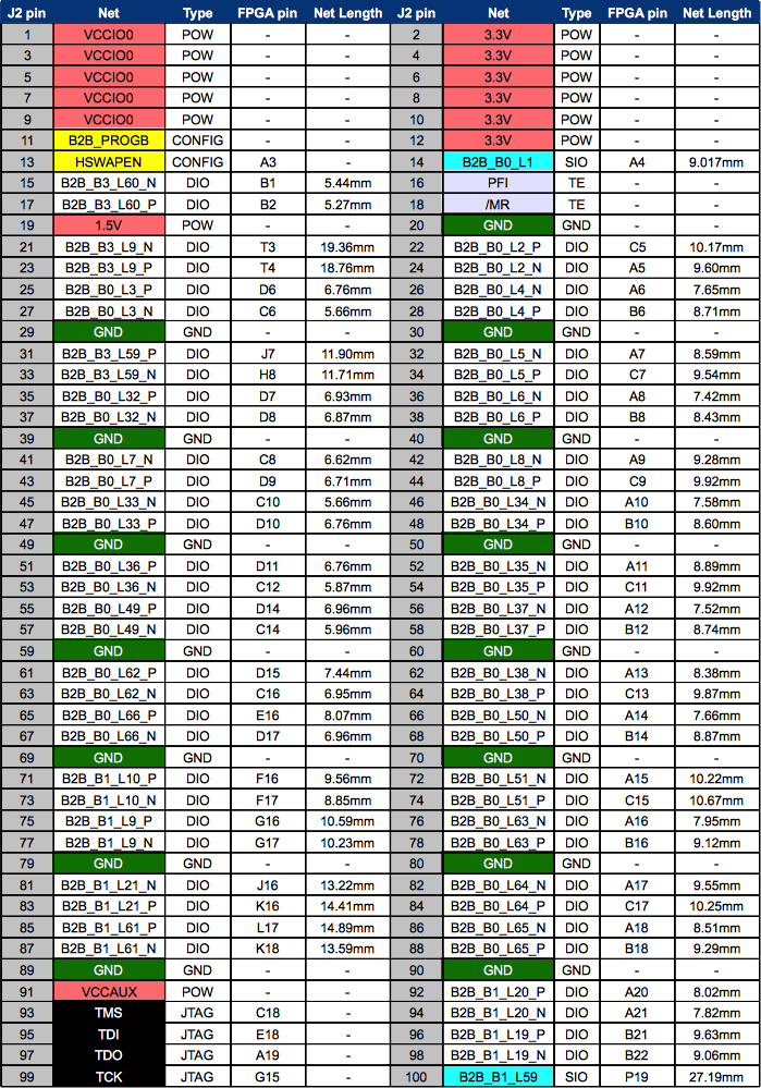
J2 Pin-out
| J2 pin | Net | Type | FPGA pin | Net Length | J2 pin | Net | Type | FPGA pin | Net Length |
| 1 | VCCIO0 | POW | - | - | 2 | 3.3V | POW | - | - |
| 3 | VCCIO0 | POW | - | - | 4 | 3.3V | POW | - | - |
| 5 | VCCIO0 | POW | - | - | 6 | 3.3V | POW | - | - |
| 7 | VCCIO0 | POW | - | - | 8 | 3.3V | POW | - | - |
| 9 | VCCIO0 | POW | - | - | 10 | 3.3V | POW | - | - |
| 11 | B2B_PROGB | CONFIG | - | - | 12 | 3.3V | POW | - | - |
| 13 | HSWAPEN | CONFIG | A3 | - | 14 | B2B_B0_L1 | SIO | A4 | 9.017mm4715mm |
| 15 | B2B_B3_L60_N | DIO | B1 | 57.44mm5418mm | 16 | PFI | TE | - | - |
| 17 | B2B_B3_L60_P | DIO | B2 | 56.27mm7655mm | 18 | /MR | TE | - | - |
| 19 | 1.5V | POW | - | - | 20 | GND | GND | - | - |
| 21 | B2B_B3_L9_N | DIO | T3 | 1921.36mm4246mm | 22 | B2B_B0_L2_P | DIO | C5 | 1012.17mm0314mm |
| 23 | B2B_B3_L9_P | DIO | T4 | 1821.76mm2943mm | 24 | B2B_B0_L2_N | DIO | A5 | 911.60mm8853mm |
| 25 | B2B_B0_L3_P | DIO | D6 | 69.76mm0158mm | 26 | B2B_B0_L4_N | DIO | A6 | 710.65mm8292mm |
| 27 | B2B_B0_L3_N | DIO | C6 | 58.66mm4466mm | 28 | B2B_B0_L4_P | DIO | B6 | 811.71mm2228mm |
| 29 | GND | GND | - | - | 30 | GND | GND | - | - |
| 31 | B2B_B3_L59_P | DIO | J7 | 1114.90mm0801mm | 32 | B2B_B0_L5_N | DIO | A7 | 811.59mm7078mm |
| 33 | B2B_B3_L59_N | DIO | H8 | 1113.71mm8896mm | 34 | B2B_B0_L5_P | DIO | C7 | 911.54mm9983mm |
| 35 | B2B_B0_L32_P | DIO | D7 | 69.93mm1276mm | 36 | B2B_B0_L6_N | DIO | A8 | 710.42mm6094mm |
| 37 | B2B_B0_L32_N | DIO | D8 | 69.87mm1646mm | 38 | B2B_B0_L6_P | DIO | B8 | 810.43mm9961mm |
| 39 | GND | GND | - | - | 40 | GND | GND | - | - |
| 41 | B2B_B0_L7_N | DIO | C8 | 69.62mm1167mm | 42 | B2B_B0_L8_N | DIO | A9 | 912.28mm2657mm |
| 43 | B2B_B0_L7_P | DIO | D9 | 69.71mm3073mm | 44 | B2B_B0_L8_P | DIO | C9 | 912.92mm5699mm |
| 45 | B2B_B0_L33_N | DIO | C10 | 58.66mm889mm | 46 | B2B_B0_L34_N | DIO | A10 | 711.58mm7216mm |
| 47 | B2B_B0_L33_P | DIO | D10 | 69.76mm1201mm | 48 | B2B_B0_L34_P | DIO | B10 | 811.60mm6163mm |
| 49 | GND | GND | - | - | 50 | GND | GND | - | - |
| 51 | B2B_B0_L36_P | DIO | D11 | 68.76mm6976mm | 52 | B2B_B0_L35_N | DIO | A11 | 812.89mm4283mm |
| 53 | B2B_B0_L36_N | DIO | C12 | 58.87mm3601mm | 54 | B2B_B0_L35_P | DIO | C11 | 912.92mm6535mm |
| 55 | B2B_B0_L49_P | DIO | D14 | 69.96mm136mm | 56 | B2B_B0_L37_N | DIO | A12 | 710.52mm7513mm |
| 57 | B2B_B0_L49_N | DIO | C14 | 58.96mm7449mm | 58 | B2B_B0_L37_P | DIO | B12 | 811.74mm0849mm |
| 59 | GND | GND | - | - | 60 | GND | GND | - | - |
| 61 | B2B_B0_L62_P | DIO | D15 | 79.44mm687mm | 62 | B2B_B0_L38_N | DIO | A13 | 812.38mm5431mm |
| 63 | B2B_B0_L62_N | DIO | C16 | 69.95mm5212mm | 64 | B2B_B0_L38_P | DIO | C13 | 912.87mm8448mm |
| 65 | B2B_B0_L66_P | DIO | E16 | 810.07mm0885mm | 66 | B2B_B0_L50_N | DIO | A14 | 711.66mm3259mm |
| 67 | B2B_B0_L66_N | DIO | D17 | 69.96mm9228mm | 68 | B2B_B0_L50_P | DIO | B14 | 811.87mm4909mm |
| 69 | GND | GND | - | - | 70 | GND | GND | - | - |
| 71 | B2B_B1_L10_P | DIO | F16 | 911.56mm3734mm | 72 | B2B_B0_L51_N | DIO | A15 | 1012.22mm0938mm |
| 73 | B2B_B1_L10_N | DIO | F17 | 811.85mm466mm | 74 | B2B_B0_L51_P | DIO | C15 | 1012.67mm5055mm |
| 75 | B2B_B1_L9_P | DIO | G16 | 1012.59mm5086mm | 76 | B2B_B0_L63_N | DIO | A16 | 711.95mm3551mm |
| 77 | B2B_B1_L9_N | DIO | G17 | 1012.23mm6008mm | 78 | B2B_B0_L63_P | DIO | B16 | 911.12mm772mm |
| 79 | GND | GND | - | - | 80 | GND | GND | - | - |
| 81 | B2B_B1_L21_N | DIO | J16 | 1315.22mm7408mm | 82 | B2B_B0_L64_N | DIO | A17 | 913.55mm5157mm |
| 83 | B2B_B1_L21_P | DIO | K16 | 1415.41mm9404mm | 84 | B2B_B0_L64_P | DIO | C17 | 1013.25mm4806mm |
| 85 | B2B_B1_L61_P | DIO | L17 | 1417.89mm852mm | 86 | B2B_B0_L65_N | DIO | A18 | 812.51mm4997mm |
| 87 | B2B_B1_L61_N | DIO | K18 | 1317.59mm4155mm | 88 | B2B_B0_L65_P | DIO | B18 | 912.29mm3889mm |
| 89 | GND | GND | - | - | 90 | GND | GND | - | - |
| 91 | VCCAUX | POW | - | - | 92 | B2B_B1_L20_P | DIO | A20 | 811.02mm0846mm |
| 93 | TMS | JTAG | C18 | - | 94 | B2B_B1_L20_N | DIO | A21 | 710.82mm7172mm |
| 95 | TDI | JTAG | E18 | - | 96 | B2B_B1_L19_P | DIO | B21 | 912.63mm0803mm |
| 97 | TDO | JTAG | A19 | - | 98 | B2B_B1_L19_N | DIO | B22 | 911.06mm8608mm |
| 99 | TCK | JTAG | G15 | - | 100 | B2B_B1_L59 | SIO | P19 | 2730.19mm179mm |
Signal Integrity Considerations
...
Traces of differential signals pairs are NOT routed with equal length, although difference in signal lines length is negligible for actual signal frequencies. For applications where traces length has to be matched or timing differences have to be compensated, Tables below abowe list the trace length of I/O signal lines measured from FPGA balls to B2B connector pins.
...
| Signal FPGA pin | BR3 R19 | BR2 P18 | BR1 N16 | BR0 P17 |
|---|---|---|---|---|
| Revision 01 | 1 | 1 | 1 | 1 |
| Revision 02 | 1 | 1 | 1 | 0 |
| Revision 03 | 1 | 1 | 0 | 1 |
| Revision 04 | 1 | 1 | 0 | 0 |
Board revisions pin coding
...
- Optimized placement and routing for DC/DC converters
- Added thermal vias to mounting holes
- Added Testpoints
- Changed Board revision identification to REV03
- Changed U9 from SIT1602AI-83-33E-25.0000 to SiT8008AI-73-XXS-25.000000E
- Added Track-it™ Traceability Pad
- Change SPI Flash from W25Q128BVEIG to W25Q128FVEIG
- DDR3 changed from IM4G16D3EABG-125I to IM4G16D3FABG-125I for the 4 GBit variants
- U13 (DS2432P+) is no longer populated by default
Main differences between 03 and 04 revisions:
- Optimized placement and routing
- More powerful regulators
- Removed stucked vias
- Added Testpoints
- Changed Board revision identification to REV04
- U12 was fitted for all module assembly variants as default
Module assembly variants coded by 4 zero ohm resistors, connected to FPGA AV[3:0] Module assembly variants coded by 4 zero ohm resistors, connected to FPGA AV[3:0] pins. All these pins should be configured to have internal PULLUP.
| Signal FPGA pin | AV3 M18 | AV2 M17 | AV1 V20 | AV0 U19 | Speed grade | SDRAM | Temp grade | Status | ||
|---|---|---|---|---|---|---|---|---|---|---|
| TE0600-02[V|B] | 0 | 0 | 0 | 0 | 2 | 2x128MBit | C | obsolete | ||
| TE0600-02[V|B]I | 0 | 0 | 0 | 1 | 2 | 2x128MBit | I | obsolete | ||
| TE0600-02[V|B]F | 0 | 0 | 1 | 0 | 3 | 2x128MBit | C | obsolete | ||
| TE0600-02[V|B]IF | 0 | 0 | 1 | 1 | 3 | 2x128MBit | I | obsolete | ||
| TE0600-02[V|B]MF | 0 | 1 | 0 | 0 | 3 | 2x512MBit | C | obsolete | ||
| TE0600-03[V|B] | 0 | 0 | 0 | 0 | 2 | 2x128MBit | C | full production | ||
| TE0600-03[V|B]I | 0 | 0 | 0 | 1 | 2 | 2x128MBit | I | full production | ||
| TE0600-03[V| | B]F0 | B]F | 0 | 0 | 1 | 0 | 3 | 2x128MBit | C | full production |
| TE0600-03[V|B]IF | 0 | 0 | 1 | 1 | 3 | 2x128MBit | I | full production | ||
| TE0600-03[V|B]MF | 0 | 1 | 0 | 0 | 3 | 2x512MBit | C | full production | ||
| TE0600-04-52I11 | 0 | 0 | 0 | 1 | 2 | 2x128MBit | I | full production | ||
| TE0600-04-72C11 | 0 | 0 | 0 | 0 | 2 | 2x128MBit | C | full production | ||
| TE0600-04-72C21 | 0 | 1 | 0 | 0 | 2 | 2x512MBit | C | full production | ||
| TE0600-04-83C21 | 0 | 1 | 01 | 0 | 3 | 2x128MBit2x512MBit | C | full production | ||
| TE0600 | -03[V|B]IF-04-83I11 | 0 | 0 | 1 | 1 | 3 | 2x128MBit | I | full production | |
| TE0600 | -03[V|B]MF-04-83I21 | 0 | 1 | 01 | 01 | 3 | 2x512MBit | CI | full production |
Assembly variants pin coding
...
Date | Revision | Contributors | Description |
|---|---|---|---|
| 2011-10-01 | 0.01 | AIK | Release. |
| 2011-10-05 | 0.02 | AIK | Added B2B pin-out section. |
| 2011-10-06 | 0.03 | AIK | Reformatted pin-out tables. Added eFUSE programming section. |
| 2011-10-06 | 0.04 | AIK | Added board photos. Additions to eFUSE section. |
| 2011-10-06 | 0.05 | AIK | Removed net length information for nets which can't be measured right. |
| 2011-10-06 | 0.06 | AIK | Added power consumption section. |
| 2011-10-08 | 0.07 | AIK | Little fixes after FDR audit. |
| 2011-10-12 | 0.08 | AIK | Fix in eFUSE section. |
| 2011-11-11 | 0.09 | AIK | Added pin numbering description for B2B connectors |
| 2012-01-20 | 0.10 | AIK | Added pin compatibility note and manual reference. |
| 2012-04-12 | 0.11 | AIK | Added FPGA banks VCCIO voltages table. |
| 2012-04-17 | 1.00 | FDR | Updated documentation link. Replaced obsolete ElDesI and RedMine links with current GitHub links. Updated dating convention. |
| 2012-05-18 | 1.01 | AIK | Corrected cross-reference in section 3.2. Corrected LED description. |
| 2012-06-18 | 1.02 | FDR | Removed junction temperature limits under connector current ratings. |
| 2012-07-18 | 1.03 | AIK | Added table with B2B signals summary per FPGA bank |
| 2012-10-30 | 2.01 | AIK | Fork to 01 and 02 board revisions |
| 2012-11-06 | 2.01 | AIK | Fixed bank 1 power options |
| 2012-11-21 | 2.02 | AIK | Updated module diagram |
| 2012-11-30 | 2.03 | AIK | Added Ethernet disable note |
| 2012-12-19 | 2.04 | AIK | Fixed SPI Flash size on block diagram |
| 2013-01-21 | 2.05 | AIK | Added PHY reset note |
| 2013-03-13 | 2.06 | AIK | Connectors current chapter moved to separate document |
| 2013-03-13 | 2.07 | AIK | Changed Bank 1 power supply description and VCCIO0 sources description |
| 2016-01-29 | 2.08 | AIK | Pause advertise correction |
| 2016-11-05 | 3.00 | FDR | Document ported to wiki and adapted to web presentation. |
| 2017-04-03 | TT | Added REV03 to assembly Variant Table | |
| 2024-03-11 | 4.00 | MT | Added REV04 to assembly variant coding table Added REV04 to revision coding table Added main differences between 03 and 04 revisions Updated nets lengths table Added info about additional 3.3V single-ended oscillator (U12) Updated supply diagram Updated block diagram |
Disclaimer
| Include Page | ||||
|---|---|---|---|---|
|
Overview
Content Tools