Page History
...
Figure 1: TE0715 block diagram.
Main Components

 Main
Main
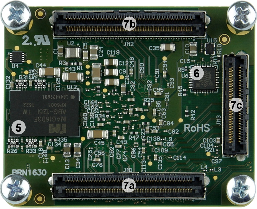
Figure 2: TE0715 main components.
...
Table 3: General overview of board to board I/O signals.
For detailed information about the pin-out, please refer to the Pin-out Table.
...
| U10 Signal | Default Frequency | Notes |
|---|---|---|
IN1/IN2 | Externally supplied | Needs decoupling on carrier board. |
IN3 | 25.000000 MHz | Reference input clock. |
IN4 | - | Wired to the GND. |
IN5/IN6 | 125 MHz | Ethernet PHY output clock. |
CLK0 A/B | - | Not used, disabled. |
CLK1 A/B | - | Not used, disabled. |
CLK2 A/B | 125 MHz | MGT reference clock 1. |
CLK3A- | 50 MHz (new firmware, see PCN) | Bank 34 clock input, default disabled, user clock. |
CLK3B | - | Not used, disabled. |
...
Overview
Content Tools