Page History
| Scroll pdf ignore | |
|---|---|
Table of Contents
|
Overview
| Scroll Only (inline) |
|---|
On https://wiki.trenz-electronic.de/display/PD/TE0714 the online version of this manual and other documents can be found. |
The Trenz Electronic TE0714 is an industrial-grade SoM (System om Module) based on Xilinx Artix-7, 16 MByte Flash memory and powerful switch-mode power supplies for all on-board voltages. A large number of configurable I/O's is provided via rugged high-speed stacking strips. All modules in 4 x 5 cm form factor are mechanically compatible.
Block diagram

Board Components
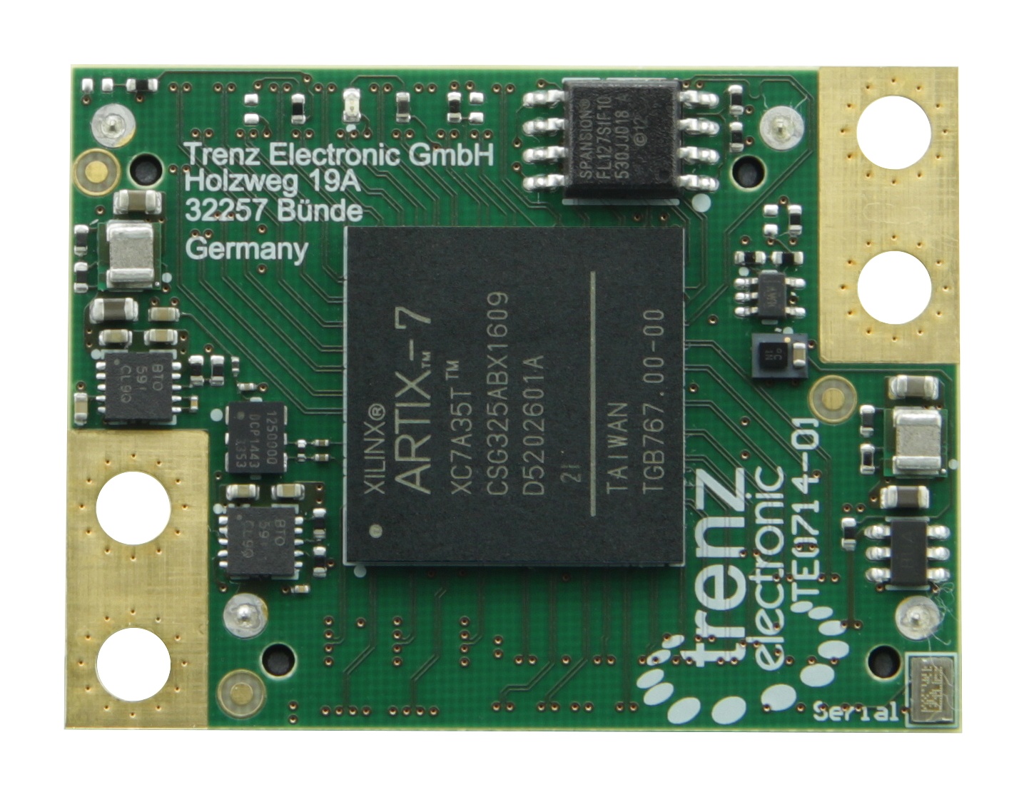 | 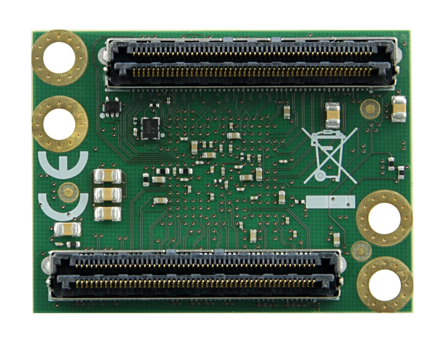 |
Top view | Bottom view |
Main Components:
Artix-7 FPGA
B2B-Connectors
- SPI Flash
- MEMS Oscillator (PL Clock)
- LVDS Oscillator (GT Clock)
- Power Supply for all on-board components
Key Features
Xilinx Artix-7 (A15T, A35T, A50T)
- Rugged for shock and high vibration
- 16 MByte QSPI Flash memory
- Differential MEMS Oscillator for GT Clocking
- MEMS Oscillator for PL Clocks (option)
- Plug-on module with 2 × 100-pin high-speed hermaphroditic strips
- 144 FPGA I/O's (max 68 differential)
- XADC Analog Input
- 4 GTP (high-performance transceiver) lanes
- GT Reference Clock input
- Optimized I/O and power pins for good signal integrity
- On-board high-efficiency DC-DC converters
- eFUSE bit-stream encryption (AES)
- One user LED
Assembly options for cost or performance optimization available upon request. Possible options:
- FPGA Type (A15T, A35T, A50T), temperature grade
- GT Clock Frequency (or none if not assembled)
- PL Clock Frequency and precision or none if not assembled)
- Config and B14 Bank Voltage: 1.8V or 3.3V
- SPI Flash type (or none if not assembled)
- LED Color (or none if not assembled)
- PUDC Pin strapping (pull high or pull down)
- GT Power Enable pin strapping (default power enabled or disabled)
Current Assembly Variants
| Variant | FPGA | GT Clock | PL Clock | PUDC | GT PWR Enable | B14/Config Voltage | SPI Flash | LED |
|---|---|---|---|---|---|---|---|---|
| Standard | A35T-2I | 125MHz | 25Mhz | Low | Enabled | 3.3V | S25FL127S | Red |
| 35-2IC6 | A35T-2I | 125MHz | 25MHz | Low | Enabled | 1.8V | N25Q128 | Red |
Signals, Interfaces and Pins
Boot Modes
Two boot modes are controlled by the MODE signal on the board to board (B2B) connector:
MODE signal | Boot Mode |
|---|---|
high or open | Master SPI, x4 Mode |
low or ground | Slave SelectMAP |
JTAG
JTAG access to the Xilinx Artix-7 device is provided through connector JM1.
Signal | B2B Pin |
|---|---|
| TCK | JM1: 89 |
| TDI | JM1: 85 |
| TDO | JM1: 87 |
| TMS | JM1: 91 |
Clocking
Clock | Default Frequency | IC | FPGA | Notes |
|---|---|---|---|---|
| CLK125MHz | 25 MHz | U8 | T14 | Frequency depends on Assembly variant |
| MGT_CLK | 125MHz | U2 | B6/B5 | Frequency depends on Assembly variant |
Peripherals
LED's
There is 1 LED on TE0714:
LED | Color | FPGA | Notes |
|---|---|---|---|
D4 | Red | K18 |
|
Power
For startup, a power supply with minimum current capability of 1A is recommended.
Power Supplies
TE0714 needs one single power supply with nominal 3.3V.
...
Power consumption measurements. Actual power consumption depends on the FPGA design and ambient temperature.
Bank Voltages
Bank | Voltage | Notes |
|---|---|---|
0 Config and B14 | 1.8V or 3.3V | Depends on assembly option |
15 | User | Supplied from base, max 3.3V |
34 | User | Supplied from base, max 3.3V |
Initial Delivery state
Storage device name | Content | Notes |
|---|---|---|
SPI Flash OTP Area | Empty, not programmed | Except serial number programmed by flash vendor |
SPI Flash Quad Enable bit | Programmed | |
SPI Flash main array | demo design | |
EFUSE USER | Not programmed | |
EFUSE Security | Not programmed |
Hardware Revision History
| PCB Revision | Changes |
|---|---|
01 | Current Hardware Revision, no changes |
Technical Specification
Absolute Maximum Ratings
Parameter | Min | Max | Units | Notes | Reference document |
|---|---|---|---|---|---|
Vin supply voltage | -0.1 | 3.6 | V | ||
| I/O Bank supply voltage | -0.5 | 3.6 | V | Xilinx document DS181 | |
| I/O input voltage for FPGA I/O banks | -0.4 | VCCO_X+0.55 | V | Xilinx document DS181 | |
| GT Transceiver | -0.5 | 1.26 | V | Xilinx document DS181 | |
Voltage on Module JTAG pins | -0.4 | VCCO_0+0.55 | V | VCCO_0 is 1.8V or 3.3V nominal | Xilinx document DS181 |
Storage Temperature | -40 | +85 | C |
Recommended Operating Conditions
| Parameter | Min | Max | Units | Notes | Reference document |
|---|---|---|---|---|---|
| Vin supply voltage | 3.135 | 3.45 | V | ||
| IO Bank supply voltage for I/O banks | 1.14 | 3.465 | V | Xilinx document DS181 | |
| I/O input voltage for I/O banks | -0.20 | Vcco + 0.20 | V | Xilinx document DS181 | |
| Voltage on Module JTAG pins | 3.135 | 3.465 | V | For assembly variant with 3.3V CONFIG Bank Option | Xilinx document DS181 |
| Note |
|---|
| Please check Xilinx Datasheet for complete list of Absolute maximum and recommended operating ratings for the Artix-7 device (DS181). |
Physical Dimensions
Module size: 40 mm × 30 mm. Please download the assembly diagram for exact numbers.
Mating height with standard connectors: 8 mm
PCB thickness: 1.6 mm
Highest part on PCB: approx. 2.5 mm. Please download the step model for exact numbers.
All dimensions are shown in mm and can be found here.
Temperature Ranges
Commercial grade modules
All parts are at least commercial temperature range of 0°C to +70°C. The module operating temperature range depends on customer design and cooling solution. Please contact us for options.
...
All parts are at least industrial temperature range of -40°C to +85°C. The module operating temperature range depends on customer design and cooling solution. Please contact us for options.
Weight
| Variant | Weight g | Note |
|---|---|---|
| 2IC6 | 8.3 | Plain Module |
Document Change History
Date | Revision | Authors | Description |
|---|---|---|---|
2016-06-01 | initial version |
Disclaimer
| Include Page | ||||
|---|---|---|---|---|
|
...
Overview
Content Tools