Page History
| scroll-ignore |
|---|
Download PDF version of this document. |
| scroll-pdf-ignore | |||
|---|---|---|---|
Table of Contents
|
Overview
| Scroll Only (inline) |
|---|
OnlineRefer to https://shop.trenz-electronic.de/de/Download/?path=Trenz_Electronic/TE0715 for online version of this manual and other related documents canavailable beabout found at https://wiki.trenz-electronic.de/display/PD/TE0715 |
...
the product. |
The Trenz Electronic TE0715 is an industrial-grade SoM (System on Module) based on Xilinx Zynq-7000 SoC (XC7Z015 or XC7Z030) with 1GB of DDR3 SDRAM, 32MB of SPI flash memory, gigabit Ethernet PHY transceiver, a USB PHY transceiver and powerful switching-mode power supplies for all on-board voltages. A large number of configurable I/Os is provided via rugged high-speed stacking strips.
Block
...
Diagram

Main
...
Components
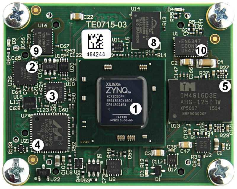

1. Zynq-7000 all programmable SoC.
...
10. PowerSoC DC-DC converter.
Key
...
Features
Industrial-grade Xilinx Zynq-7000 (XC7Z015, XC7Z030) SoM
- Rugged for shock and high vibration
- 2 × ARM Cortex-A9
- 10/100/1000 tri-speed gigabit Ethernet transceiver PHY
- MAC address EEPROM
- 32-Bit wide 1GB DDR3 SDRAM
- 32 MByte QSPI flash memory
- Programmable clock generator
- Transceiver clock (default 125 MHz)
- Plug-on module with 2 × 100-pin and 1 × 60-pin high-speed hermaphroditic strips
- 132 FPGA I/Os (65 LVDS pairs possible) and 14 PS MIO available on B2B connectors
- 4 GTP/GTX (high-performance transceiver) lanes
- GTP/GTX (high-performance transceiver) clock input
- USB 2.0 high-speed ULPI transceiver
- On-board high-efficiency DC-DC converters
- 4.0 A x 1.0 V power rail
- 1.5 A x 1.5 V power rail
- 1.5 A x 1.8 V power rail
- System management
- eFUSE bit-stream encryption
- AES bit-stream encryption
- Temperature compensated RTC (real-time clock)
- User LED
- Evenly-spread supply pins for good signal integrity
...
Storage device name | Content | Notes |
|---|---|---|
24AA025E48 EEPROM | User content not programmed | Valid MAC Address from manufacturer. |
SPI Flash OTP Area | Empty, not programmed | Except serial number programmed by flash vendor. |
SPI Flash Quad Enable bit | Programmed | - |
SPI Flash main array | Demo design | - |
EFUSE USER | Not programmed | - |
EFUSE Security | Not programmed | - |
Signals, Interfaces and Pins
Board to Board (B2B) I/O's
...
For detailed information about the pin out, please refer to the Master Pinout TableTables.
Default MIO Mapping
| MIO | Function | B2B Pin | Notes | MIO | Function | B2B Pin | Notes | |
|---|---|---|---|---|---|---|---|---|
| 0 | GPIO | JM1-87 | B2B | 16..27 | ETH0 | - | RGMII | |
| 1 | QSPI0 | - | SPI Flash-CS | 28..39 | USB0 | - | ULPI | |
| 2 | QSPI0 | - | SPI Flash-DQ0 | 40 | SDIO0 | JM1-27 | B2B | |
| 3 | QSPI0 | - | SPI Flash-DQ1 | 41 | SDIO0 | JM1-25 | B2B | |
| 4 | QSPI0 | - | SPI Flash-DQ2 | 42 | SDIO0 | JM1-23 | B2B | |
| 5 | QSPI0 | - | SPI Flash-DQ3 | 43 | SDIO0 | JM1-21 | B2B | |
| 6 | QSPI0 | - | SPI Flash-SCK | 44 | SDIO0 | JM1-19 | B2B | |
| 7 | GPIO | - | Green LED D4 | 45 | SDIO0 | JM1-17 | B2B | |
| 8 | QSPI0 | - | SPI Flash-SCKFB | 46 | GPIO | - | Ethernet PHY LED2 INTn Signal. | |
| 9 | JM1-91 | B2B | 47 | GPIO | - | RTC Interrupt | ||
| 10 | JM1-95 | B2B | 48 | I2C1 | - | SCL on-board I2C | ||
| 11 | JM1-93 | B2B | 49 | I2C1 | - | SDA on-board I2C | ||
| 12 | JM1-99 | B2B | 50 | GPIO | - | ETH0 Reset | ||
| 13 | JM1-97 | B2B | 51 | GPIO | - | USB Reset | ||
| 14 | UART0 | JM1-92 | B2B | 52 | ETH0 | - | MDC | |
| 15 | UART0 | JM1-85 | B2B | 53 | ETH0 | - | MDIO |
...
| Pin Name | Mode | Function | Default Configuration |
|---|---|---|---|
| EN1 | Input | Power Enable | No hard wired function on PCB, when forced low pulls POR_B low to emulate power on reset. |
| PGOOD | Output | Power Good | Active high when all on-module power supplies are working properly. |
| NOSEQ | - | - | No function. |
| RESIN | Input | Reset | Active low reset, gated to POR_B. |
| JTAGEN | Input | JTAG Select | Low for normal operation. |
Boot
...
Modes
By default the TE-0715 supports QSPI and SD Card boot modes which is controlled by the MODE input signal from the B2B connector.
...
| I/O | Default Frequency | Notes |
|---|---|---|
IN1/IN2 | Externally supplied | Needs decoupling on base board. |
IN3 | 25MHz | Fixed input clock. |
IN4 | - | - |
IN5/IN6 | 125MHz | Ethernet PHY output clock. |
CLK0 | - | Not used, disabled. |
CLK1 | - | Not used, disabled. |
CLK2 A/B | 125MHz | MGT reference clock 1. |
CLK3A | 125MHz | Bank 34 clock input. |
CLK3B | - | Not used, disabled. |
MAC
...
Address EEPROM
A Microchip 24AA025E48 EEPROM (U19) is used which contains a globally unique 48-bit node address, that is compatible with EUI-48(TM) and EUI-64(TM) specification. The device is organized as two blocks of 128 x 8-bit memory. One of the blocks stores the 48-bit node address and is write protected, the other block is available for application use. It is accessible through the I2C slave address 0x50.
...
Bank | Schematic Name | Voltage | TE0715-xx-15 | TE0715-xx-30 |
|---|---|---|---|---|
| 500 | VCCO_MIO0_500 | 3.3V | - | - |
| 501 | VCCO_MIO1_501 | 1.8V | - | - |
| 502 | VCCO_DDR_502 | 1.5V | - | - |
| 0 Config | VCCO_0 | 3.3V | - | - |
| 13 HR | VCCO_13 | User | HR: 1.2V to 3.3V | HR: 1.2V to 3.3V |
| 34 HR/HP | VCCO_34 | User | HR: 1.2V to 3.3V | HP: 1.2V to 1.8V |
| 35 HR/HP | VCCO_35 | User | HR: 1.2V to 3.3V | HP: 1.2V to 1.8V |
Board to Board Connectors
| Include Page | ||||
|---|---|---|---|---|
|
Technical Specifications
...
Absolute Maximum Ratings
Parameter | Min | Max | Units | Notes | Reference Document|||||
|---|---|---|---|---|---|---|---|---|---|
VIN supply voltage 2 | -0. | 53 | 56. | 50 | V | - | |||
3.3VIN supply voltage 3 | -0. | 1354 | 3. | 4656 | V | - | |||
| VBat | VBAT_INsupply voltage | 2.7 | 5.5-1 | 6.0 | V | - | |||
| PL | I/OIO bank supply voltage for HR | I/O banks (VCCO) | 1-0. | 145 | 3. | 4656 | V | - | Xilinx datasheet DS191 | PL I/O
PL IO bank supply voltage for HP | I/O banks (VCCO) | 1-0. | 145 | 12. | 890 | V | TE0715-xx-15 does not have | HP banks. | Xilinx datasheet DS191 |
| I/O input voltage for HR I/O banks | (*) | (*) | V | (*) Check datasheet | -0.4 | VCCO_X+0.55 | V | - | |
| I/O input voltage for HP I/O banks | (*) | (*)-0.55 | VCCO_X+0.55 | V | TE0715-xx-15 does not have | HP banks. | |||
| GT receiver ( | *) Check datasheetXilinx datasheet DS191RXP/RXN) and transmitter (TXP/TXN) | -0.5 | 1.26 | V | - | ||||
Voltage on | Module module JTAG pins | 3-0. | 1354 | VCCO_0+0.55 | 3.465V | VCCO_0 is 3. | 3 V3V nominal. |
Absolute Maximum Ratings
Storage temperature | -40 | +85 | °C | - |
| Storage temperature without the ISL12020MIRZ | -55 | +100 | °C | - |
| Note |
|---|
| Assembly variants for higher storage temperature range are available on request. |
| Note |
|---|
| Please check Xilinx datasheet DS187 (for XC7Z015) or DS191 (for XC7Z030) for complete list of absolute maximum and recommended operating ratings. |
Recommended Operating Conditions
| Parameter | Min | Max | Units | Notes | Reference Document | |||
|---|---|---|---|---|---|---|---|---|
| VIN supply voltage | 2.5 | 5.5 | V | |||||
| 3.3VIN supply voltage | 3.135 | 3.465 | V | |||||
| VBAT_IN supply voltage | 2.7 | 5.5 | V | |||||
PL I/O bank supply voltage for HR I/O banks (VCCO) | 1.14 | 3.465 | V | Xilinx datasheet DS191 | ||||
PL I/O bank supply voltage for HP I/O banks (VCCO) | 1.14 | 1.89 | ||||||
Parameter | Min | Max | Units | Notes | ||||
VIN supply voltage | -0.3 | 6.0 | V | - | ||||
3.3VIN supply voltage | -0.4 | 3.6 | V | - | ||||
| VBat supply voltage | -1 | 6.0 | V | - | ||||
| PL IO bank supply voltage for HR I/O banks (VCCO) | -0.5 | 3.6 | V | - | ||||
PL IO bank supply voltage for HP I/O banks (VCCO) | -0.5 | 2.0 | V | TE0715-xx-15 does not have HP banks. | ||||
| I/O input voltage for HR I/O banks | -0.4 | VCCO_X+0.55 | V | - | ||||
| I/O input voltage for HP I/O banks | -0.55 | VCCO_X+0.55V | TE0715-xx-15 does not have HP banks | .|||||
| GT receiver (RXP/RXN) and transmitter (TXP/TXN) | -0.5 | 1.26 | V | - | ||||
| Xilinx datasheet DS191 | ||||||||
| I/O input voltage for HR I/O banks | (*) | (*) | V | (*) Check datasheet | Xilinx datasheet DS191 or DS187 | |||
| I/O input voltage for HP I/O banks | (*) | (*) | V | TE0715-xx-15 does not have HP banks (*) Check datasheet | Xilinx datasheet DS191 | |||
| Voltage on Module JTAG pins | 3.135 | 3.465 | Voltage on module JTAG pins | -0.4 | VCCO_0+0.55V | VCCO_0 is 3. | 3V3 V nominal | .|
Storage temperature | -40 | +85 | °C | - | ||||
| Storage temperature without the ISL12020MIRZ | -55 | +100 | °C | - |
| Note |
|---|
| Assembly variants for higher storage temperature range are available on request. |
| Note |
|---|
| Please check Xilinx datasheet DS187 (for XC7Z015) or DS191 (for XC7Z030) for complete list of absolute maximum and recommended operating ratings. |
Physical Dimensions
Physical Dimensions
Module size: 50 mm × 40 Module size: 50 mm × 40 mm. Please download the assembly diagram for exact numbers
Mating height with standard connectors: 8mm
PCB thickness: 1.6mm
Highest part on PCB: approx. 2.5mm. Please download the step model for exact numbers
...
8.8 g - Set of bolts and nuts
...
Revision History
Hardware Revision History
| Date | Revision | Contributors | Description | 2016-10-18 | A.N.: added table "power rails" | Notes | PCN | Documentation link | |
|---|---|---|---|---|---|---|---|---|---|
| 2016-06-21 | 04 | Second production release | Click to see PCN | TE0715 | |||||
| - | 03 | First production release | TE0715-03 | ||||||
| - | 02 | Prototypes | |||||||
| - | 01 | Prototypes |
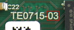
Hardware revision number is printed on the PCB board together with the module model number separated by the dash.
Document Change History
Date | Revision | Contributors | Description |
|---|---|---|---|
| 2016-11-15 | Thorsten Trenz
| Added B2B Connector section | |
| 2016-10-18 | V40 | Ali Naseri | Added table "power rails" |
| 2016-06-28 | V38
| ||
| 2016-06-28 | V38
| Philipp Bernhardt, Antti Lukats, Thorsten Trenz, Emmanuel Vassilakis, Jan Kumann | New overall document layout with shorter table of contents. Revision 01 PCB pictures replaced with the revision 03 ones. Fixed link to Master Pinout Table. New default MIO mapping table design. Revised Power-on section. Added links to related Xilinx online documents. Physical dimensions pictures revised. Revision number picture with explanation added. |
| 2016-04-27 | V33 | Philipp Bernhardt, Antti Lukats, Thorsten Trenz, Emmanuel Vassilakis | Added the table "Recommended Operating Conditions" Storage Temperature edited. |
| 2016-03-31 | V10 | Philipp Bernhardt, Antti Lukats, Thorsten Trenz | Initial version. |
Hardware Revision History
...
Notes
...
01
...
Prototypes
...
, Emmanuel Vassilakis, Jan Kumann | New overall document layout with shorter table of contents. Revision 01 PCB pictures replaced with the revision 03 ones. Fixed link to Master Pinout Table. New default MIO mapping table design. Revised Power-on section. Added links to related Xilinx online documents. Physical dimensions pictures revised. Revision number picture with explanation added. | ||
| 2016-04-27 | V33 | Philipp Bernhardt, Antti Lukats, Thorsten Trenz, Emmanuel Vassilakis | Added the table "Recommended Operating Conditions" Storage Temperature edited. |
| 2016-03-31 | V10 | Initial version. |
Hardware revision number is printed on the PCB board together with the module model number separated by the dash.
...
Disclaimer
| Include Page | ||||
|---|---|---|---|---|
|
Overview
Content Tools