Page History
...
The Trenz Electronic TE0714 is an industrial-grade SoM (System on Module) based on Xilinx Artix-7, 16 MByte Mbyte Flash memory and powerful switching mode power supplies for all on-board voltages. A large number of configurable I/O's is provided via rugged high-speed stacking strips. All modules in 4 x 5 cm form factor are mechanically compatible.
Block
...
Diagram

Board Components
|
|
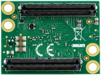
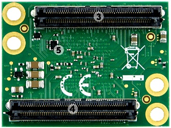
Top view | Bottom view |
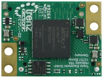
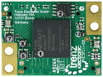
Main Components:
- Artix-7 FPGA, U4
- SPI Flash, U7
- B2B
...
- Connector, JM2
- B2B Connector, JM1
...
- MEMS Oscillator (PL Clock), U8
- Single Output Low-Dropout Linear Regulator, U6 (1.2V_MGT)
- Single Output Low-Dropout Linear Regulator, U5 (1.0V_MGT)
- Low-Jitter Precision LVDS Oscillator (GT Clock), U2
- Red Indication LED,D4
- Step-Down DC-DC Converter, U1 (1.0V)
...
- PFET Load Switch With Configurable Slew Rate, Q1 (3.3V)
- Low Power Step-Down DC-DC Converter, U3 (1.8V)
- Voltage Detector for Circuit Initialization and Timing Supervision, U23
Key Features
Xilinx Artix-7 (A15T, A35T, A50T)
- Rugged for shock Sock and high vibrationHigh Vibration
- 16 MByte QSPI Flash memoryMemory
- Differential MEMS Oscillator for GT Clocking
- MEMS Oscillator for PL Clocks (optionOptional)
- Plug-on module with On Module With 2 × 100-pin high-speed hermaphroditic stripsPin High-Speed Hermaphroditic Strips
- 144 FPGA I/O's (max Max 68 differentialDifferential)
- XADC Analog Input
- 4 GTP (highHigh-performance transceiverPerformance Transceiver) lanesLanes
- GT Reference Clock inputInput
- Optimized I/O and power pins for good signal integrityPower Pins for Good Signal Integrity
- On-board highHigh-efficiency Efficiency DC-DC convertersConverters
- Power Supply for All On-Board Components
- eFUSE bitBit-stream encryption Stream Encryption (AES)
- One user User Configurable LED
Assembly options for cost or performance optimization available upon request. Possible options:
- FPGA Type (A15T, A35T, A50T), temperature grade
- GT Clock Frequency (or none if not assembled)
- PL Clock Frequency and precision (or none if not assembled)
- Config and B14 Bank Voltage: 1.8V or 3.3V
- SPI Flash type (or none if not assembled)
- LED Color (or none if not assembled)
- PUDC Pin strapping (pull high or pull down)
- GT Power Enable pin strapping (default power enabled or disabled)
Current Assembly Variants
| Variant | FPGA | GT Clock [MHz] | PL Clock [MHz] | PUDC | GT PWR Enable | B14/Config Voltage [V] | R27 (VCCIO_0 on JM2 Pin 54) | SPI Flash | LED |
|---|---|---|---|---|---|---|---|---|---|
| TE0714-02-35-2I | A35T-2I | 125 | 25 | High | Enabled | 3.3 | JM2 Pin 54 = VCCIO_0 (3.3 V) | S25FL127S | Red |
| TE0714-02-35-2IC6 | A35T-2I | 125 | 25 | High | Enabled | 1.8 | JM2 Pin 54 = Open | N25Q128 | Red |
| TE0714-02-35-2IC7 | A35T-2I | 125 | 25 | Low | Enabled | 3.3 | JM2 Pin 54 = Open | S25FL127S | Red |
| TE0714-02-50-2I | A50T-2I | 125 | 25 | High | Enabled | 3.3 | JM2 Pin 54 = VCCIO_0 (3.3 V) | S25FL127S | Red |
| TE0714-02-50-2IC6 | A50T-2I | 125 | 25 | High | Enabled | 1.8 | JM2 Pin 54 = Open | N25Q128 | Red |
| Note |
|---|
On REV 01 JM2 Pin 54 was connected to GND. When R27 is not populated, REV 02 is backwards compatible to REV 01. When R27 is set, check your baseboard to not connect this pin to GND. For all new baseboards JM2.54 should be used as VCCIO output (it will then be 1.8V or 3.3V depending the voltage settings on the module. |
Signals, Interfaces and Pins
...
| Note |
|---|
SPI D2 and D3 have no pull-ups on the module so with PUDC=High option, those pins are floating if there are no pull-ups on baseboard. As those pins have SPI RESET function when Quad mode is not enabled, it is mandatory to either add pull-ups on user baseboard or program the Quad Enable bit in Flash nonvolatile status register. |
JTAG Interface
JTAG access to the Xilinx Artix-7 device is provided through connector JM1.
Signal Name | B2B Pin |
|---|---|
| TCK | JM1: 89 |
| TDI | JM1: 85 |
| TDO | JM1: 87 |
| TMS | JM1: 91 |
Clocking
Clock | Default Frequency | IC | FPGA | Notes |
|---|---|---|---|---|
| CLK125MHz | 25 MHz | U8 | T14 | Frequency depends on Assembly variant |
| MGT_CLK | 125MHz | U2 | B6/B5 | Frequency depends on Assembly variant |
...
LED's
There is 1 one LED on TE0714 module:
LED | Color | FPGA | Notes |
|---|---|---|---|
D4 | Red | K18 |
|
...
TE0714 needs one single power supply with nominal of 3.3V.
| Test Condition (25C ambient) | Vin Current mA | Notes |
|---|---|---|
| TE0714-35, TEBT0714, empty design, GT not enabled | 110mA |
Power consumption measurements. Actual power consumption depends on the FPGA design and ambient temperature.
Bank Voltages
Bank | Voltage | Notes |
|---|---|---|
0 Config and B14 | 1.8V or 3.3V | Depends on assembly option |
15 | User | Supplied from base, max 3.3V |
34 | User | Supplied from base, max 3.3V |
...
| PCB Revision | Changes | PCN link | Documentation link |
|---|---|---|---|
01 | Current Hardware Revision, no changes | - | TE0714-01 TRM |
| 02 | VCCIO0 added to B2B | PCN-20160815 | - |
...
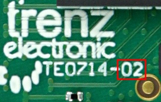
Hardware revision number is printed on the PCB board next to the module model number separated by the dash.
Technical Specifications
Absolute Maximum Ratings
Parameter | Min | Max | Units | Notes | Reference document |
|---|---|---|---|---|---|
Vin supply voltage | -0.1 | 3.6 | V | ||
| I/O Bank supply voltage | -0.5 | 3.6 | V | Xilinx document DS181 | |
| I/O input voltage for FPGA I/O banks | -0.4 | VCCO_X+0.55 | V | Xilinx document DS181 | |
| GT Transceiver | -0.5 | 1.26 | V | Xilinx document DS181 | |
Voltage on Module JTAG pins | -0.4 | VCCO_0+0.55 | V | VCCO_0 is 1.8V or 3.3V nominal | Xilinx document DS181 |
Storage Temperature | -40 | +85 | C |
Recommended Operating Conditions
| Parameter | Min | Max | Units | Notes | Reference document |
|---|---|---|---|---|---|
| Vin supply voltage | 3.135 | 3.45 | V | ||
| IO Bank supply voltage for I/O banks | 1.14 | 3.465 | V | Xilinx document DS181 | |
| I/O input voltage for I/O banks | -0.20 | Vcco + 0.20 | V | Xilinx document DS181 | |
| Voltage on Module JTAG pins | 3.135 | 3.465 | V | For assembly variant with 3.3V CONFIG Bank Option | Xilinx document DS181 |
...
Weight
| Variant | Weight g | Note |
|---|---|---|
| 2IC6 | 8.3 | Plain Module |
Document Change History
...
| Include Page | ||||
|---|---|---|---|---|
|
Overview
Content Tools