Page History
...
Block Diagram

Main Components
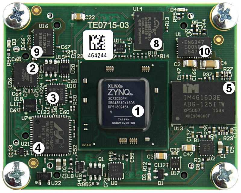


- 1.
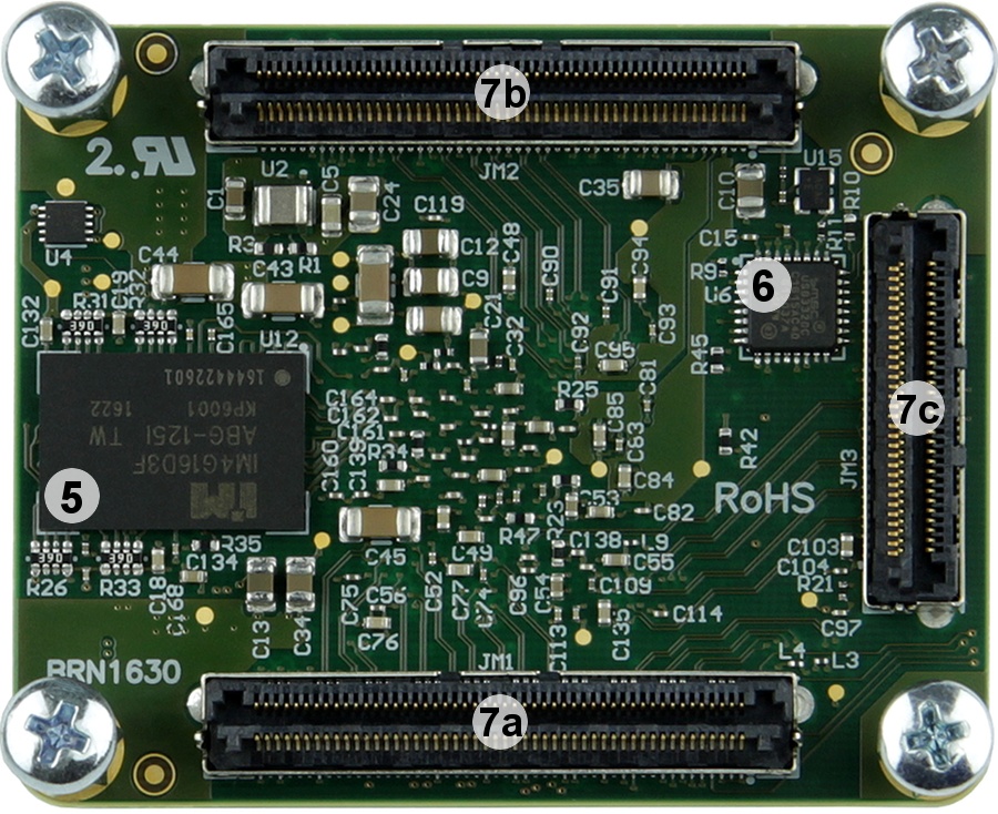
...
- Xilinx Zynq-7000
...
- All Programmable SoC, U5
- 2. System
...
- Controller CPLD
...
- , U26
...
- 3. Programmable
...
- Quad Clock Generator , U10
- 4. 10/100/1000 Mbps Ethernet PHY
...
- , U7
...
- 5.
...
- 4 Gbit DDR3L SDRAM (1.35 V), U12 and U13
- 6. Hi-Speed USB 2.0 ULPI transceiver
...
- , U6
...
- 7a. B2B connector Samtec Razor Beam™ LSHM-150, JM1
...
...
- 7b. B2B connector
...
- Samtec Razor Beam™ LSHM-150, JM2
- 7c. B2B connector Samtec Razor Beam™ LSHM-130, JM3
...
...
- 8.
...
- 32-MByte Quad SPI Flash memory, U14
- 9. Low power RTC
...
- With Battery Backed SRAM, U16
- 10.
...
- 4A PowerSoC DC-DC Converter, U1
- 11. Green LED (DONE), D2
- 12. Red LED (SC), D3
- 13. Green LED (MIO7), D4
- 14. 2-Bit Bidirectional 1-MHz I2C Bus Voltage-Level Translator, U20
Key Features
Industrial-grade Xilinx Zynq-7000 (XC7Z015, XC7Z030) SoM
- Rugged for shock and high vibration
- 2 × ARM Cortex-A9
- 10/100/1000 tri-speed gigabit Mbps Ethernet transceiver PHY
- MAC address EEPROM
- 32-Bit wide 1GB DDR3 SDRAM
- 32 MByte QSPI flash memory
- Programmable clock generator
- Transceiver clock (default 125 MHz)
- Plug-on module with 2 × 100-pin and 1 × 60-pin high-speed hermaphroditic strips
- 132 FPGA I/Os (65 LVDS pairs possible) and 14 PS MIO available on B2B connectors
- 4 GTP/GTX (high-performance transceiver) lanes
- GTP/GTX (high-performance transceiver) clock input
- USB 2.0 high-speed ULPI transceiver
- On-board high-efficiency DC-DC converters
- 4.0 A x 1.0 V power rail
- 1.5 A x 1.5 V power rail
- 1.5 A x 1.8 V power rail
- System management
- eFUSE bit-stream encryption
- AES bit-stream encryption
- Temperature compensated RTC (real-time clock)
- User LED
- Evenly-spread supply pins for good signal integrity
...
Signals, Interfaces and Pins
Board to Board (B2B) I/
...
Os
I/O signals connected to the SoC's I/O bank and B2B connector:
...
For detailed information about the pin out, please refer to the Pinout TablesPin-out Table.
Default MIO Mapping
| MIO | Function | B2B Pin | Notes | MIO | Function | B2B Pin | Notes | |
|---|---|---|---|---|---|---|---|---|
| 0 | GPIO | JM1-87 | B2B | 16..27 | ETH0 | - | RGMII | |
| 1 | QSPI0 | - | SPI Flash-CS | 28..39 | USB0 | - | ULPI | |
| 2 | QSPI0 | - | SPI Flash-DQ0 | 40 | SDIO0 | JM1-27 | B2B | |
| 3 | QSPI0 | - | SPI Flash-DQ1 | 41 | SDIO0 | JM1-25 | B2B | |
| 4 | QSPI0 | - | SPI Flash-DQ2 | 42 | SDIO0 | JM1-23 | B2B | |
| 5 | QSPI0 | - | SPI Flash-DQ3 | 43 | SDIO0 | JM1-21 | B2B | |
| 6 | QSPI0 | - | SPI Flash-SCK | 44 | SDIO0 | JM1-19 | B2B | |
| 7 | GPIO | - | Green LED D4 | 45 | SDIO0 | JM1-17 | B2B | |
| 8 | QSPI0 | - | SPI Flash-SCKFB | 46 | GPIO | - | Ethernet PHY LED2 INTn Signal. | |
| 9 | JM1-91 | B2B | 47 | GPIO | - | RTC Interrupt | ||
| 10 | JM1-95 | B2B | 48 | I2C1 | - | SCL on-board I2C | ||
| 11 | JM1-93 | B2B | 49 | I2C1 | - | SDA on-board I2C | ||
| 12 | JM1-99 | B2B | 50 | GPIO | - | ETH0 Reset | ||
| 13 | JM1-97 | B2B | 51 | GPIO | - | USB Reset | ||
| 14 | UART0 | JM1-92 | B2B | 52 | ETH0 | - | MDC | |
| 15 | UART0 | JM1-85 | B2B | 53 | ETH0 | - | MDIO |
...
MODE Signal State | Boot Mode |
|---|---|
high High or open | SD Card |
low Low or ground | QSPI |
...
LEDs
| LED | Color | Connected to | Description and Notes |
|---|---|---|---|
D2 | Green | DONE | Reflects inverted DONE signal, ON when FPGA is not configured, OFF as soon as PL is configured. This LED will not operate if the SC can not power on the 3.3V output rail that also powers the 3.3V circuitry on the module. |
D3 | Red | SC | System main status LED. |
D4 | Green | MIO7 | User controlled, default OFF (when PS7 has not been booted). |
...
On-board Peripherals
Processing System (PS) Peripherals
...
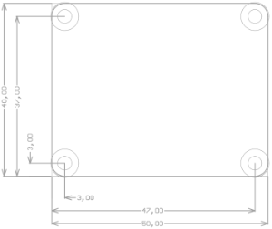
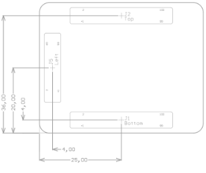
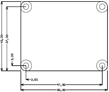
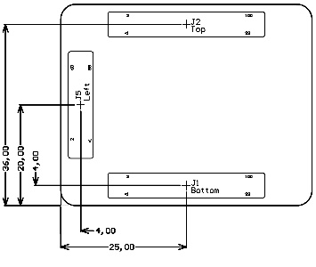
All dimensions are given in mm.
Operating Temperature Ranges
...
| Date | Revision | Notes | PCN | Documentation link |
|---|---|---|---|---|
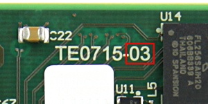
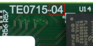
| 2016-06-21 | 04 | Second production release | Click to see PCN | TE0715-04 |
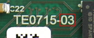
| - | 03 | First production release | TE0715-03 | |
| - | 02 | Prototypes | TE0715-02 | |
| - | 01 | Prototypes |
Hardware revision number is printed on the PCB board together with the module model number separated by the dash.
Document Change History
Date | Revision | Contributors | Description |
|---|---|---|---|
| 2017-01-14 | Jan Kumann | Product revision 04 images added. Formatting changes and small corrections. | |
| 2016-11-15 | V45 | Thorsten Trenz | Added B2B Connector section. |
| 2016-10-18 | V40 | Ali Naseri | Added table "power rails". |
| 2016-06-28 | V38
| Philipp Bernhardt, Antti Lukats, Thorsten Trenz, Emmanuel Vassilakis, Jan Kumann | New overall document layout with shorter table of contents. Revision 01 PCB pictures replaced with the revision 03 ones. Fixed link to Master Pin-out Table. New default MIO mapping table design. Revised Power-on section. Added links to related Xilinx online documents. Physical dimensions pictures revised. Revision number picture with explanation added. |
| 2016-04-27 | V33 | Thorsten Trenz, Emmanuel Vassilakis | Added table "Recommended Operating Conditions". Storage Temperature edited. |
| 2016-03-31 | V10 | Philipp Bernhardt, Antti Lukats | Initial version. |
...
Overview
Content Tools