Page History
...
| Scroll Only (inline) |
|---|
Refer to https://shop.trenz-electronic.de/de/Download/?path=Trenz_Electronic/carrier_boards/TEBA0841 for downloadable version of this manual and additional technical documentation of the product. |
The Trenz Electronic TE0705 TEBA0841 Carrier Board is a base-board for 4x5 SoMs, which exposes the MIOis dedicated for test- and the PS/PL-pins of the SoM to accessible connectors and provides a whole range of on-board components to test and evaluate evaluate-purposes of Multi-gigabit transceiver units of Trenz Electronic 4x5 SoMs.
See page "4 x 5 cm carriers" to get information about the SoMs supported by the TE0705 TEBA0841 Carrier Board.
Block Diagram
Figure 1: TE0705TEBA0841-04 01 Block Diagram
Main Components
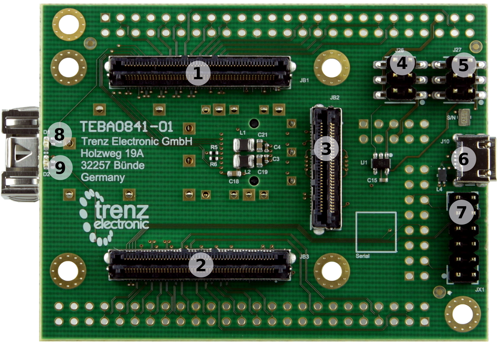
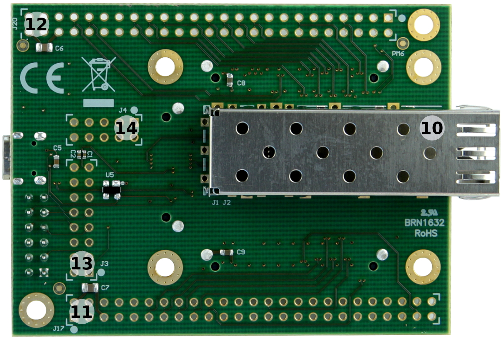
Figure 2: 4x5 SoM carrier board TE0705TEBA0841-0401
TE0705TEBA0841-0401:
- ARM JTAG Connector (DS-5 D-Stream) J15 - PJTAG to EMIO multiplexing needed
- 12-pin IDC header socket J1 (right angle, max. VCCIO-voltage: 3.3V): mapped to 8 Zynq PS MIO0-bank-pins (MIO0, MIO9 to MIO15), 6 pins (MIO10 to MIO15) are additionally connected to TE0705 System-Controller-CPLD
RJ45 GbE Connector
- SD Card Socket - Zynq SDIO0 Bootable SD port
- 12-pin IDC header socket (right angle) J2 for access to Zynq-module's PL IO-bank pins (not usable as LVDS-pairs, only single-ended IOs, max. VCCIO-voltage: VIOTB)
- Micro USB Connector J12 (Device, Host or OTG Modes)
- Battery holder for CR1220 (RTC backup voltage)
- 12-pin IDC header socket (vertical) J5 for access to Zynq-module's PL IO-bank pins (4 LVDS-pairs, max. VCCIO-voltage: VIOTB)
- 12-pin IDC header socket (vertical) J6 for access to Zynq-module's PL IO-bank pins (4 LVDS-pairs, max. VCCIO-voltage: VIOTB)
- User Push-Button S2 ("RESTART" button by default)
- User Push-Button S1 ("RESET" button by default)
- User LEDs D6, D7, D8, D9 (function mapping depends on firmware of System-Controller-CPLD)
- User LEDs D4, D5, D14, D15 (same as above)
- Mini USB Connector (USB JTAG and UART Interface) J7
- User 4-bit DIP-Switch S3
- User 4-bit DIP-Switch S4
- FTDI FT2232HQ USB 2.0 High Speed to UART/FIFO
- Lattice Semiconductor MachXO2 1200HC System-Controller-CPLD
- Jumper J4 to fix user button S2 to switched state
- 40-Pin-Header J13 for access to PL IO-bank-pins
- 40-Pin-Header J11 for access to PL IO-bank-pins
- Samtec Razor Beam™ high-speed hermaphroditic 50 positions terminal strip, board to board connector, JB1
- Samtec Razor Beam™ high-speed hermaphroditic 50 positions terminal strip, board to board connector, JB2
- Samtec Razor Beam™ high-speed hermaphroditic 50 positions terminal strip, board to board connector, JB3
- Barrel jack for 12V Power Supply J10
- Jumper J21 to select supply voltage VIOTB
- Jumper J9, J19, J20 to select supply voltage USB-VBUS
Key Features
- Samtec Razor Beam™ LSHM-150 B2B connector JB1
- Samtec Razor Beam™ LSHM-150 B2B connector JB3
- Samtec Razor Beam™ LSHM-130 B2B connector JB2
- 6-pin header J26 for selecting VCCIOA supply-voltage
- 6-pin header J27 for selecting VCCIOD supply-voltage
- Micro USB Connector J12 (Device or OTG mode)
- JTAG header, connected to JTAG interface of 4x5 Module (XMOD FTDI JTAG Adapter compatible pin assigment)
- User LED D1 (green)
- User LED D2 (red)
- SFP+ Connector J1
- 50-pin header soldering-pads J17 for access to SoM's IO-banks (LVDS-pairs possible)
- 50-pin header soldering-pads J20 for access to SoM's IO-banks (LVDS-pairs possible)
- 16-pin header soldering-pads J3, XMOD FTDI JTAG Adapter compatible pin assigment with 2 additional pins for reference-clock input to 4x5 SoM
- 10-pin header soldering-pads J4 for access to SoM's SDIO-port (voltage translation via SDIO Port Expander necessary)
Key Features
- SFP+ connector (Enhanced small form-factor pluggable), supports data transmission rates up to 10 Gbit/s
- Micro-USB-Interface (J10) connected to Zynq-module (Device or OTG mode)
- Trenz 4x5 module Socket (3 x Samtec LSHM series connectors)
- 4x5 SoM programable by JTAG header (JX1)
- 2 x user LEDs routed to MIO-pins of the SoM
- Soldering-pads J17 and J20 as place-holder for further possibilities to access to SoMs IO-bank-pins, usable as LVDS-pairs
- Overvoltage-, undervoltage- and reversed- supply-voltage-protection
- Barrel jack for 12V power supply
- Carrier Board System-Controller-CPLD Lattice MachXO2 1200HC, programable by Mini-USB JTAG-Interface J7
- Zynq-module programable by ARM-JTAG-Interface-Connector (J15) or by System-Controller-CPLD via Mini-USB JTAG-Interface J7
- RJ45 Gigabit Ethernet MagJack with 2 integrated LEDs
- 2x 40-Pin-Header J11 and J13 for access to Zynq-module's PL IO-bank-pins, operable with fixed (3.3V) or adjustable IO-voltage VIOTB (not usable as LVDS-pairs, only single-ended IOs)
- USB JTAG- and UART-Interface (FTDI FT2232HQ) with Mini-USB-Connector J7
- 8 x user LEDs routed to System-Controller-CPLD, 8 x red
- 2 x user-push button routed to System-Controller-CPLD; by default configured as system "RESET" and "RESTART" button (depends on CPLD-Firmware)
- 2 x 4-bit DIP-Switch for base-board-configuration (3 switches routed to System-Controller-CPLD, 3 switches to set voltage FMC_VADJ, 1 switch routed to Zynq-module (MIO0), 1 switch enables Mini-USB JTAG-Interface J7)
- 12-pin IDC header socket (vertical) J5, J6 for access to Zynq-module's LVDS-pairs (max. VCCIO-voltage: VIOTB)
- 12-pin IDC header socket (right angle) J1 for access to Zynq-module's MIO0-bank-pins MIO0, MIO9 ... MIO15 (J1-6 (MIO12) buffered by Schmitt-Trigger-Buffer (5.0V Hysteresis), else max. VCCIO-voltage 3.3V)
- 12-pin IDC header socket (right angle) J2 for access to Zynq-module's PL IO-bank-pins (max. VCCIO-voltage: VIOTB)
- Micro SD card socket, can be used to boot system
- Micro-USB-Interface (J12) connected to Zynq-module (Device, Host or OTG modes)
- Trenz 4x5 module Socket (3 x Samtec LSHM series connectors)Soldering-pads J3 and J4 as place-holder for access to JTAG- or SDIO-port of the SoM
Interfaces and Pins
Micro SD Card Socket
...
On the TE0705 Carrier Board there is a 4-bit DIP-switch S3 (see (15) in Figure 1) available. The default switch mapping is as follows:
| Switch | Functionality |
|---|---|
| S3-1 | CM1: Mode pin 1 (routed to Carrier Controller) |
| S3-2 | CM0: Mode pin 0 (routed to Carrier Controller) |
| S3-3 | JTAGEN: Set to ON for normal JTAG operation. Must be moved to OFF position for TE0705 System-Controller-CPLD update only |
| S3-4 | MIO0: Readable signal by System-Controller-CPLD and mounted TE07xx Module |
4-bit DIP-switch S4
Additionally, on the TE0705 Carrier Board there is a 4-bit DIP-switch S3 (see (16) in Figure 1) available. The signals of the switch are routed to carrier board's System-Controller-CPLD and are fully user-configurable depending on a customer developed CPLD-firmware. Please refer to the documentation of the TE0705 System-Controller-CPLD to get information how to put these user-switches in operation.
...
On the TE0705 Carrier Board there are two push buttons (S1 and S2) and are routed to the System-Controller-CPLD and available to the user. The default mapping of the push buttons is as follows:
| Name | Default Mapping: | ||
|---|---|---|---|
| S1 | If S1 is pushed, the active-low RESet IN (RESIN) signal will be asserted. Note: This reset can also be forced by the FTDI USB-to-JTAG interface. | ||
| S2 | If S2 is pushed, the active-high Power ON (PON) signal (that is internally pulled-up) will be deasserted, which can be considered as a "RESTART" button to switch off (push button) and on (release button) all on-module power supplies (except 3.3VIN). Note: The capability of the switch to be enabled the first time will become active shortly after Power on Reset (POR).
By closing jumper J4 the PON-signal will be permanently deasserted, hence the power FET switch and the DC-DC converters on module will be disabled. |
The functionality of the push buttons depends on the CPLD-firmware. For detailed information of the function of the push buttons, please refer to the documentation of the TE0705 System-Controller-CPLD.
...
Note: The configuration of VADJ depends on the used firmware of the System-Controller-CPLD. For detailed information, refer to the documentation of the TE0705 System-Controller-CPLD.
S3-1 (CM1) | S3-2 (CM2) | VADJ Value |
|---|---|---|
OFF | OFF | 1.8V |
OFF | ON | 2.5V |
ON | OFF | 3.3V |
ON | ON | 1.8V (Note: Also Zynq-module's SC-CPLD JTAG-access is enabled, see section JTAG in the documentation of the TE0705 System-Controller-CPLD.) |
Table 3: Switch S3 positions for fixed values of the VADJ voltage
...
On the TE0705 carrier board all PL IO-bank's supply voltages of the 4x5 SoM (VCCIOA, VCCIOB, VCCIOC, VCCIOD; see 4x5 Module Integration Guide) are connected to the VCCIO-voltage VIOTB, which is either fixed to 3.3V (J21: 1-2, 3) or selectable with the adjustable supply-voltage VADJ (J21: 1, 2-3). The supply-voltages have following pin assignments on B2B-connectors:
base-board supply-voltages | base-board B2B connector-pins | standard assignment of PL IO-bank supply-voltages on TE 4x5 module's B2B connectors | base-board voltages and signals connected with |
|---|---|---|---|
| VIOTB | JB1-10, JB1-12, JB2-2, JB2-4, JB2-6, JB2-8, JB2-10 | VCCIOA (JM1-9, JM1-11), VCCIOB (JM2-1, JM2-3), VCCIOC (JM2-5), VCCIOD (JM2-7, JM2-9) | VCCIO3 (Systm-Controller-CPLD pin 5, 11, 23), J15 VTREF, J11, J13, J2, J5 and J6 VCCIO |
Table 4: base-board supply-voltage VIOTB
| Note |
|---|
Note: The corresponding PL IO-voltage supply voltages of the 4x5 SoM to the selectable base-board voltage VIOTB are depending on the mounted 4x5 SoM and varying in order of the used model. Refer to SoM's schematic to get information about the specific pin assignment on module's B2B-connectors regarding PL IO-bank supply voltages and to the 4x5 Module integration Guide for VCCIO voltage options. |
Following table describes how to configure the base-board supply-voltages by jumpers:
base-board supply-voltages vs voltage-levels | VIOTB | USB-VBUS |
|---|---|---|
| 3V3 | J21:1-2, 3 | - |
| VADJ | J21:1, 2-3 | - |
| 5V0 intern | - | J9:1-2, 3 & J19: 1-2 (J20: 1-2: additional decoupling-capacitor 100 µF) |
| Vbus extern | - | J9: 1, 2-3 & J19: open |
Table 5: Configuration of base-board supply-voltages via jumpers. Jumper-Notification: 'Jx: 1-2, 3' means pins 1 and 2 are connected, 3 is open. 'Jx: 1, 2-3' means pins 2 and 3 are connected, 1 is open
| Note |
|---|
| It is recommended to set and measure the PL IO-bank supply-voltages before mounting of TE 4x5 module to avoid failures and damages to the functionality of the mounted SoM. |
...
On the TE0705 the 5.0V and 3.3V power supply rails are generated by high performance DC-DC-converters from the external 12V supply. While the 3.3V plane supplies several on-board components (e.g., Lattice CPLD and FTDI Dual USB UART/FIFO IC), the 5V plane is mainly provided to power supply of the module to be carried (e.g., TE0720 Zynq SoC module). For the latter, however, special considerations must be taken (see TE0720 Power Supply). Therefore, the on-module system controller (SC) must be provided with information about the power-on-reset (POR) process, namely, the following control signals EN1, RESIN, and NOSEQ. And the SC provides, in turn, the status signal PGOOD down to the on-board System-Controller-CPLD.
| Signal | Description | ||
|---|---|---|---|
| EN1 | This CPLD output active-high signal is a “power on (PON)” signal that is usually HIGH (weak pull-up), except, the user push button S2 is pressed, which forces the related signal to be LOW (ground). EN1 enables (EN1=’1’) and disables (EN1=’0’) the power supplies on the carried module, respectively. | ||
| RESIN | This signal is controlled by the user push button S1 on the TE0701 and is forwarded directly to the SC, where it is latched together with the EN1 signal as well as the “all power rails OK” signal (1.0V and 1.8V for core; 1.5V and VTT for RAM, and 3.3V).
When RESIN (alias user push button S1) is not pushed and simultaneously the EN1 signal is asserted (EN='1') and all power rails are ok, the active-high Zynq power-on-reset signal PS_POR_B is asserted. | ||
| NOSEQ | This CPLD signal can be used to enable or disable the power sequencing mode. If the active-high NOSEQ signal is set to HIGH (NOSEQ='1') then the 1.0V and 1.8V power supplies on the carried module will be forced to be enabled. In normal mode (NOSEQ='0') the 3.3V power supply is turned on after the 1.0V and 1.8V supplies have stabilized (see TE0720 Power Supply). The latter is the default mode, i.e., for the NOSEQ pin of the SC the internal pull-down is activated. After booting, the NOSEQ pin can be used as general-purpose I/O pin. For example, the SC (REV 0.02) maps the Ethernet PHY LED0 to NOSEQ by default. However, this mapping can be changed by software after boot. | ||
| PGOOD | This active-high signal (with internal pull-up) is a status input to the CPLD about the current status of the power supply rails on the carried module (e.g., TE0720). It is routed to user LED3, which is switched on when the on-module power supply rails are not ok. |
Table 6: Generation of PGOOD-signal
...
Technical Specifications
Absolute Maximum Ratings
| Parameter | Min | Max | Units | Notes |
|---|---|---|---|---|
Vin supply voltage | 11.4 | 12.6 | V | 12.0V supply voltage ± 5% |
Storage Temperature | -55 | 125 | °C | Lattice MachX02 family data sheet |
Recommended Operating Conditions
| Parameter | Min | Max | Units | Notes |
|---|---|---|---|---|
| Vin supply voltage | 11.4 | 12.6 | V | - |
Physical Dimensions
Board size: PCB 170.4 mm × 98 mm. Notice that some parts the are hanging slightly over the edge of the PCB like the mini USB-jacks (ca. 1.4 mm) and the Ethernet RJ-45 jack (ca 2.2 mm), which determine the total physical dimensions of the carrier board. Please download the assembly diagram for exact numbers.
Mating height of the module with standard connectors: 8mm
PCB thickness: ca. 1.65mm
Highest part on the PCB is the Ethernet RJ-45 jack, which has an approximately 17 mm overall hight. Please download the step model for exact numbers.
...
ca. 110 g - Plain board
Document Change History
| date | revision | authors | description |
|---|---|---|---|
| 2017-01-18 | Ali Naseri | current TRM for TE0705-04 | |
| 2017-01-15 | 0.1 | Ali Naseri | Initial document |
Hardware Revision History
| Date | Revision | Notes | PCN | Documentation link |
|---|---|---|---|---|
| 2016-10-04 | 04 | |||
| - | 03 | |||
| - | 02 | |||
| - | 01 |
Figure 5: Hardware revision Number
...
Overview
Content Tools