Page History
...
| Scroll Only (inline) |
|---|
Refer to "https://shopwiki.trenz-electronic.de/en/Download/?path=Trenz_Electronic/TE0715"display/PD/TE0715+TRM for downloadableonline version of this manual and the rest of available documentation. |
The Trenz Electronic TE0715 is an industrial-grade SoM (System on Module) based on Xilinx Zynq-7000 SoC (XC7Z015 or XC7Z030) with 1GB of DDR3 SDRAM, 32MB of SPI flash memory, gigabit Ethernet PHY transceiver, a USB PHY transceiver and powerful switching-mode power supplies for all on-board voltages. A large number of configurable I/Os is provided via rugged high-speed stacking strips.
Block Diagram
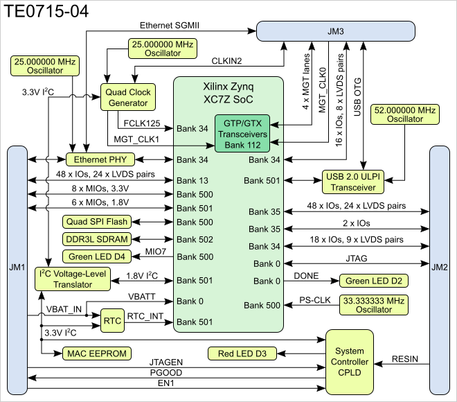
Main Components

Key Features
Industrial-grade
1.Xilinx Zynq-7000
All Programmable SoC, U5- 2. System Controller CPLD, U26
- 3. Programmable Quad Clock Generator , U10
- 4. 10/100/1000 Mbps Ethernet PHY, U7
- 5. 4 Gbit DDR3L SDRAM (1.35 V), U12 and U13
- 6. Hi-Speed USB 2.0 ULPI transceiver, U6
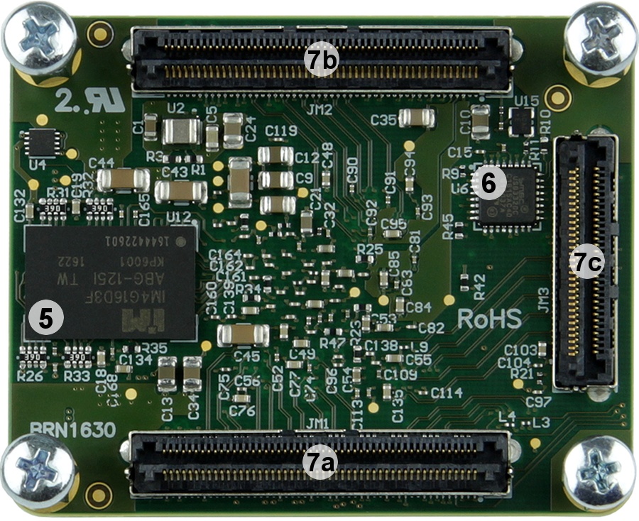
- 7a. B2B connector Samtec Razor Beam™ LSHM-150, JM1
- 7b. B2B connector Samtec Razor Beam™ LSHM-150, JM2
- 7c. B2B connector Samtec Razor Beam™ LSHM-130, JM3
- 8. 32-MByte Quad SPI Flash memory, U14
- 9. Low power RTC With Battery Backed SRAM, U16
- 10. 4A PowerSoC DC-DC Converter, U1
- 11. Green LED (DONE), D2
- 12. Red LED (SC), D3
- 13. Green LED (MIO7), D4
- 14. 2-Bit Bidirectional 1-MHz I2C Bus Voltage-Level Translator, U20
Key Features
Industrial-grade Xilinx Zynq-7000 (XC7Z015, XC7Z030) SoM
- Rugged for shock and high vibration
- 2 × ARM Cortex-A9
- 10/100/1000 Mbps Ethernet transceiver PHY
- MAC address EEPROM
- 32-Bit wide 1GB DDR3 SDRAM
- 32 MByte QSPI flash memory
- Programmable clock generator
- Transceiver clock (default 125 MHz)
- Plug-on module with 2 × 100-pin and 1 × 60-pin high-speed hermaphroditic strips
- 132 FPGA I/Os (65 LVDS pairs possible) and 14 PS MIO available on B2B connectors
- 4 GTP/GTX (high-performance transceiver) lanes
- GTP/GTX (high-performance transceiver) clock input
- USB 2.0 high-speed ULPI transceiver
- On-board high-efficiency DC-DC converters
- 4.0 A x 1.0 V power rail
- 1.5 A x 1.5 V power rail
- 1.5 A x 1.8 V power rail
- System management
- eFUSE bit-stream encryption
- AES bit-stream encryption
- Temperature compensated RTC (real-time clock)
- User LED
- Evenly-spread supply pins for good signal integrity
(XC7Z015, XC7Z030) SoC
- Rugged for shock and high vibration
- 2 × ARM Cortex-A9
- 10/100/1000 Mbps Ethernet transceiver PHY
- MAC address EEPROM
- 32-Bit wide 1GB DDR3 SDRAM
- 32 MByte QSPI flash memory
- Programmable clock generator
- Transceiver clock (default 125 MHz)
- Plug-on module with 2 × 100-pin and 1 × 60-pin high-speed hermaphroditic strips
- 132 FPGA I/Os (65 LVDS pairs possible) and 14 PS MIO available on B2B connectors
- 4 GTP/GTX (high-performance transceiver) lanes
- GTP/GTX (high-performance transceiver) clock input
- USB 2.0 high-speed ULPI transceiver
- On-board high-efficiency DC-DC converters
- 4.0 A x 1.0 V power rail
- 1.5 A x 1.5 V power rail
- 1.5 A x 1.8 V power rail
- System management
- eFUSE bit-stream encryption
- AES bit-stream encryption
- Temperature compensated RTC (real-time clock)
- User LED
- Evenly-spread supply pins for good signal integrity
Additional assembly options are available for cost or performance optimization upon request.
Block Diagram
Main Components
- 1. Xilinx Zynq-7000 all programmable SoC, U5
- 2. System Controller CPLD, U26
- 3. Programmable quad clock generator , U10
- 4. 10/100/1000 Mbps Ethernet PHY, U7
- 5. 4 Gbit DDR3L SDRAM (1.35 V), U12 and U13
- 6. Hi-speed USB 2.0 ULPI transceiver, U6
- 7a. B2B connector Samtec Razor Beam™ LSHM-150, JM1
- 7b. B2B connector Samtec Razor Beam™ LSHM-150, JM2
- 7c. B2B connector Samtec Razor Beam™ LSHM-130, JM3
- 8. 32-MByte quad SPI Flash memory, U14
- 9. Low-power RTC with battery backed SRAM, U16
- 10. 4A PowerSoC DC-DC converter, U1
- 11. Green LED (DONE), D2
- 12. Red LED (SC), D3
- 13. Green LED (MIO7), D4
- 14. 2-bit bidirectional 1-MHz I2C bus voltage-level translator, U20
| Page break |
|---|
Initial Delivery State
Storage device name | Content | Notes |
|---|---|---|
24AA025E48 EEPROM | User content not programmed | Valid MAC Address from manufacturer. |
SPI Flash OTP Area | Empty, not programmed | Except serial number programmed by flash vendor. |
SPI Flash Quad Enable bit | Programmed | - |
SPI Flash main array | Demo design | - |
eFUSE USER | Not programmed | - |
eFUSE Security | Not programmed | - |
| Si5338 OTP NVM | Default settings pre-programmed | OTP not reprogrammable re-programmable after delivery from factory |
...
| Note |
|---|
| JTAGEN pin in B2B connector JM1 should be kept low or grounded for normal operation. |
| Page break |
|---|
System Controller I/O Pins
...
| Pin Name | Mode | Function | Default Configuration |
|---|---|---|---|
| EN1 | Input | Power Enable | No hard wired function on PCB, when forced low pulls POR_B low to emulate power on reset. |
| PGOOD | Output | Power Good | Active high when all on-module power supplies are working properly. |
| NOSEQ | - | - | No function. |
| RESIN | Input | Reset | Active low reset, gated to POR_B. |
| JTAGEN | Input | JTAG Select | Low for normal operation. |
On-board LEDs
| LED | Color | Connected to | Description and Notes |
|---|---|---|---|
D2 | Green | DONE | Reflects inverted DONE signal. ON when FPGA is not configured, OFF as soon as PL is configured. This LED will not operate if the SC can not power on the 3.3V output rail that also powers the 3.3V circuitry on the module. |
D3 | Red | SC | System main status LED. |
D4 | Green | MIO7 | User controlled, default OFF (when PS7 has not been booted). |
Default MIO Mapping
Clocking
| Clock Signal | Frequency | IC | FPGA | Notes |
|---|---|---|---|---|
PS CLK | 33.3333 MHz | U11 | PS_CLK | PS subsystem main clock. |
ETH PHY reference | 25.000000 MHz | U9 | - | - |
USB PHY reference | 52.000000 MHz | U15 | - | - |
PLL reference | 25.000000 MHz | U18 | - | - |
GT REFCLK0 | - | B2B | U9/V9 | Externally supplied from baseboard. |
GT REFCLK1 | 125 MHz | U10 Si5338 | U5/V5 | Default clock is 125 MHz. |
| Page break |
|---|
Default MIO Mapping
| MIO | Function | B2B Pin | Notes | MIO | Function | B2B Pin | Notes | |||||||||
|---|---|---|---|---|---|---|---|---|---|---|---|---|---|---|---|---|
| 0 | GPIO | JM1-87 | B2B | 16..27 | ETH0 | - | RGMII | |||||||||
| 1 | ||||||||||||||||
| MIO | Function | B2B Pin | Notes | MIO | Function | B2B Pin | Notes | |||||||||
| 0 | GPIO | JM1-87 | B2B | 16..27 | ETH0 | - | RGMII | |||||||||
| 1 | QSPI0 | - | SPI Flash-CS | 28..39 | USB0 | - | ULPI | |||||||||
| 2 | QSPI0 | - | SPI Flash-DQ0 | 40 | SDIO0 | JM1-27 | B2B | |||||||||
| 3 | QSPI0 | - | SPI Flash-DQ1 | 41 | SDIO0 | JM1-25 | B2B | |||||||||
| 4 | QSPI0 | - | SPI Flash-DQ2 | 42 | SDIO0 | JM1-23 | B2B | |||||||||
| 5 | QSPI0 | - | SPI Flash-DQ3CS | 43 | SDIO0 | 28..39 | USB0 | - | ULPI | |||||||
| 2 | JM1-21 | B2B | 6 | QSPI0 | - | SPI Flash-SCKDQ0 | 4440 | SDIO0 | JM1-1927 | B2B | ||||||
| 73 | GPIOQSPI0 | - | Green LED D4SPI Flash-DQ1 | 4541 | SDIO0 | JM1-1725 | B2B | |||||||||
| 84 | QSPI0 | - | SPI Flash-SCKFBDQ2 | 4642 | GPIOSDIO0 | JM1- | Ethernet PHY LED2 INTn Signal. | 23 | B2B | |||||||
| 5 | QSPI0 | - | SPI Flash-DQ3 | 943 | SDIO0 | JM1- | 9121 | B2B | ||||||||
| 6 | 47QSPI0 | GPIO- | SPI Flash-SCK | RTC Interrupt | 1044 | SDIO0 | JM1- | 9519 | B2B | |||||||
| 7 | 48GPIO | I2C1- | - | SCL on-board I2C | Green LED D4 | 45 | SDIO0 | 11 | JM1- | 9317 | B2B | |||||
| 8 | 49QSPI0 | I2C1 | - | SDA on-board I2C | SPI Flash-SCKFB | 46 | 12 | JM1-99 | B2B | 50 | GPIO | - | Ethernet PHY LED2 INTn Signal. | |||
| 9 | ETH0 Reset | 13 | JM1-9791 | B2B | 5147 | GPIO | - | USB ResetRTC Interrupt | ||||||||
| 10 | UART0JM1- | 9295 | B2B | 5248 | ETH0I2C1 | - | MDC | 15 | UART0SCL on-board I2C | |||||||
| 11 | JM1- | 8593 | B2B | 5349 | ETH0I2C1 | - | SDA on-board I2C | |||||||||
| 12 | JM1-99 | B2B | 50 | GPIO | - | ETH0 Reset | ||||||||||
| 13 | JM1-97 | B2B | 51 | GPIO | - | USB Reset | ||||||||||
| 14 | UART0 | JM1-92 | B2B | 52 | ETH0 | - | MDC | |||||||||
| 15 | UART0 | JM1-85 | B2B | 53 | ETH0 | - | MDIO |
Gigabit Ethernet
On-board Gigabit Ethernet PHY is provided with Marvell Alaska 88E1512 IC (U7). The Ethernet PHY RGMII Interface interface is connected to the Zynq Ethernet0 PS GEM0. I/O voltage is fixed at 1.8V for HSTL signalingsignalling. SGMII (SFP copper or fiber) can be used directly with the Ethernet PHY, as the SGMII pins are available on the B2B connector JM3. The reference clock input of the PHY is supplied from an on-board 25MHz board 25.000000 MHz oscillator (U9), the 125MHz output clock signal CLK_125MHZ is connected to the IN5 pin of the PLL chip (U10).
Ethernet PHY connection
| PHY Pin | ZYNQ PS | ZYNQ PL | Notes |
|---|---|---|---|
| MDC/MDIO | MIO52, MIO53 | - | - |
| LED0 | - | J3 | Can be routed via PL to any free PL I/O pin in B2B connector. |
| LED1 | - | K8 | Can be routed via PL to any free PL I/O pin in B2B connector. This LED is connected to PL via level-shifter implemented in system controller CPLD. |
| LED2/Interrupt | MIO46 | - | - |
| CONFIG | - | - | By default the PHY address is strapped to 0x00, alternate configuration is possible. |
| RESETn | MIO50 | - | - |
| RGMII | MIO16..MIO27 | - | - |
| SGMII | - | - | on Routed to B2B connector JM3. |
| MDI | - | - | on Routed to B2B connector JM1. |
USB Interface
USB PHY is provided by USB3320 from Microchip. The ULPI interface is connected to the Zynq PS USB0. The I/O Voltage is fixed at 1.8V. The reference clock input of the PHY is supplied from an on-board 25 52.000000 MHz oscillator (U15).
USB PHY connection
| PHY Pin | ZYNQ Pin | B2B Name | Notes |
|---|---|---|---|
| ULPI | MIO28..39 | - | Zynq USB0 MIO pins are connected to the PHY. |
| REFCLK | - | - | 52MHz 52.000000 MHz from on board oscillator (U15). |
| REFSEL[0..2] | - | - | Reference clock frequency select, all set to GND selects 52MHz52.000000 MHz. |
| RESETB | MIO51 | - | Active low reset. |
| CLKOUT | MIO36 | - | Connected to 1.8V, selects reference clock operation mode. |
| DP, DM | - | OTG_D_P, OTG_D_N | USB data lines. |
| CPEN | - | VBUS_V_EN | External USB power switch active high enable signal. |
| VBUS | - | USB_VBUS | Connect to USB VBUS via a series of resistors, see reference schematics. |
| ID | - | OTG_ID | For an A-Device device connect to the ground, for a B-Device left device leave floating. |
The schematics for the USB connector and required components is different depending on the USB usage. USB standard A or B connectors can be used for Host host or Device device modes. A Mini mini-USB connector can be used for USB Device device mode. A micro-USB Micro connector can be used for Device device mode, OTG Mode mode or Host Modehost mode.
I2C Interface
On-board I2C I2C devices are connected to MIO48 and MIO49 which are configured as I2C1 by default. I2C I2C addresses for on-board devices are listed in the table below:
| I2C I2C Device | I2C I2C Address | Notes |
|---|---|---|
| EEPROM | 0x50 | |
| RTC | 0x6F | |
| Battery backed RAM | 0x57 | Integrated into RTC. |
PLL | 0x70 |
Boot
...
Process
By default the TE-0715 supports QSPI and SD Card boot modes which is controlled by the MODE input signal from the B2B JM1 connector.
MODE Signal State | Boot Mode |
|---|---|
High or open | QSPI |
Low or ground | SD Card |
On-board Peripherals
Processing System (PS) Peripherals
...
Temperature compensated RTC.
...
Clocking
...
PS CLK
...
33.3333 MHz
...
U11
...
PS_CLK
...
PS subsystem main clock.
...
ETH PHY reference
...
25 MHz
...
U9
...
-
...
USB PHY reference
...
52 MHz
...
U15
...
-
...
PLL reference
...
25 MHz
...
U18
...
-
...
GT REFCLK0
...
-
...
B2B
...
U9/V9
...
Externally supplied from baseboard.
...
GT REFCLK1
...
125 MHz
...
U10 Si5338
...
U5/V5
...
32 MByte Quad SPI Flash Memory
On-board QSPI flash memory S25FL256S (U14) is used to store initial FPGA configuration. Besides FPGA configuration, remaining free flash memory can be used for user application and data storage. All four SPI data lines are connected to the FPGA allowing x1, x2 or x4 data bus widths. Maximum data rate depends on the selected bus width and clock frequency used.
| Note |
|---|
SPI Flash QE (Quad Enable) bit must be set to high or FPGA is unable to load its configuration from flash during power-on. By default this bit is set to high at the manufacturing plant. |
Processing System (PS) Peripherals
| Name | IC | ID | PS7 | MIO | Notes |
|---|---|---|---|---|---|
| SPI Flash | S25FL256SAGBHI20 | U14 | QSPI0 | MIO1..MIO6 | |
| EEPROM I2C | 24AA025E48 | U19 | I2C1 | MIO48, MIO49 | EEPROM for MAC address. |
| RTC | ISL2020 | U16 | I2C1 | MIO48, MIO49 | Temperature compensated RTC. |
| RTC Interrupt | ISL2020 | U16 | GPIO | MIO47 | Real Time Clock interrupt. |
| Clock PLL | Si5338 | U10 | I2C1 | MIO48, MIO49 | Low jitter phase locked loop. |
| LED | - | D4 | GPIO | MIO7 | |
| USB | USB3320 | U6 | USB0 | MIO28..MIO39 | |
| USB Reset | - | - | GPIO | MIO51 | |
| Ethernet | 88E1512 | U7 | ETH0 | MIO16..MIO27 | |
| Ethernet Reset | - | - | GPIO | MIO50 |
Clocking
RTC - Real Time Clock
An temperature compensated Intersil ISL12020M is used for Real Time Clock (U16). Battery voltage must be supplied to the module from the main boardbaseboard. Battery backed registers can be accessed over I2C I2C bus at slave address of 0x6F. General purpose RAM is at I2C I2C slave address 0x57. RTC IC is supported by Linux so it can be used as hwclock device.
PLL - Phase-Locked Loop
There is a Silicon Labs I2C I2C programmable clock generator Si5338A (U10) chip on the module. It's output frequencies can be programmed using the I2C I2C bus address 0x70.
PLL connection
| I/O | Default Frequency | Notes |
|---|---|---|
IN1/IN2 | Externally supplied | Needs decoupling on base board. |
IN3 | 25MHz25.000000 MHz | Fixed input clock. |
IN4 | - | - |
IN5/IN6 | 125MHz | Ethernet PHY output clock. |
CLK0 | - | Not used, disabled. |
CLK1 | - | Not used, disabled. |
CLK2 A/B | 125MHz | MGT reference clock 1. |
CLK3A | - | Bank 34 clock input, default disabled, User clock. |
CLK3B | - | Not used, disabled. |
...
A Microchip 24AA025E48 EEPROM (U19) is used which contains a globally unique 48-bit node address, that is compatible with EUI-48(TM) and EUI-64(TM) 48TM specification. The device is organized as two blocks of 128 x 8-bit memory. One of the blocks stores the 48-bit node address and is write protected, the other block is available for application use. It is accessible through the I2C I2C slave address 0x50.
Power and Power-On Sequence
...
See Xilinx datasheet DS187 (for XC7Z015) or DS191 (for XC7Z030) for additional information. User should also check related baseboard documentation when choosing baseboard design for TE0715 module.
| Page break |
|---|
Power Rails
Voltages on B2B Name Connectors | B2B JM1 PinPins | B2B JM2 -PinPins | Input/Direction Output | Note |
|---|---|---|---|---|
| VIN | 1, 3, 5 | 2, 4, 6, 8 | Input | Supply voltage. |
| 3.3VIN | 13, 15 | - | Input | Supply voltage. |
| VCCIO13 | 9, 11 | - | Input | High range bank voltage. |
| VCCIO34 | - | 5 | Input | TE0715-xx-15: high range bank voltage. TE0715-xx-30: high performance bank voltage. |
| VCCIO35 | - | 7, 9 | Input | TE0715-xx-15: high range bank voltage. TE0715-xx-30: high performance bank voltage. |
| VBAT_IN | 79 | - | Input | RTC battery-buffer supply voltage. |
| 3.3V | - | 10, 12 | Output | Internal 3.3V voltage level. |
| 1.8V | 39 | - | Output | Internal 1.8V voltage level. |
| DDR_PWR | - | 19 | Output | Internal 1.5V or 1.35V voltage level, depends on revision. |
| VREF_JTAG | 91 | Output | JTAG reference voltage (3.3V). |
...
| Note |
|---|
| Please check Xilinx datasheet DS187 (for XC7Z015) or DS191 (for XC7Z030) for complete list of absolute maximum and recommended operating ratings. |
| Page break |
|---|
Recommended Operating Conditions
| Parameter | Min | Max | Units | Notes | Reference Document |
|---|---|---|---|---|---|
| VIN supply voltage | 2.5 | 5.5 | V | ||
| 3.3VIN supply voltage | 3.135 | 3.465 | V | ||
| VBAT_IN supply voltage | 2.7 | 5.5 | V | ||
PL I/O bank supply voltage for HR I/O banks (VCCO) | 1.14 | 3.465 | V | Xilinx datasheet DS191 | |
PL I/O bank supply voltage for HP I/O banks (VCCO) | 1.14 | 1.89 | V | TE0715-xx-15 does not have HP banks | Xilinx datasheet DS191 |
| I/O input voltage for HR I/O banks | (*) | (*) | V | (*) Check datasheet | Xilinx datasheet DS191 or DS187 |
| I/O input voltage for HP I/O banks | (*) | (*) | V | TE0715-xx-15 does not have HP banks (*) Check datasheet | Xilinx datasheet DS191 |
| Voltage on Module JTAG pins | 3.135 | 3.465 | V | VCCO_0 is 3.3 V nominal |
| Page break |
|---|
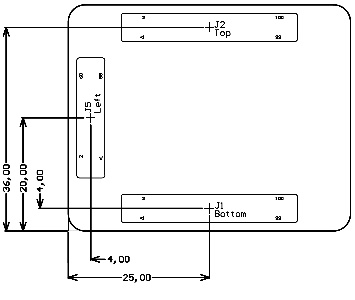
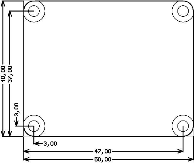
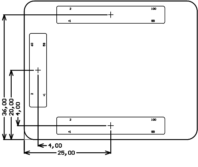
Physical Dimensions
Module size: 50 mm × 40 mm. Please download the assembly diagram for exact numbers
Mating height with standard connectors: 8mm
PCB thickness: 1.6mm
Highest part on PCB: approx. 2.5mm. Please download the step model for exact numbers
All dimensions are given in millimeters.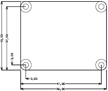
Operating Temperature Ranges
...
Hardware Revision History
| Date | Revision | Notes | Link to PCN | Documentation Link |
|---|---|---|---|---|
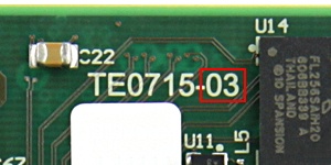
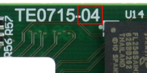
| 2016-06-21 | 04 | Second production release | Click to see PCN | TE0715-04 |
| - | 03 | First production release | TE0715-03 | |
| - | 02 | Prototypes | TE0715-02 | |
| - | 01 | Prototypes |
Hardware revision number is printed on the PCB board together with the module model number separated by the dash.
Document Change History
Date | Revision | Contributors | Description |
|---|---|---|---|
| 2017-03-02 | Thorsten Trenz | Corrected boot mode table | |
| 2017-02-10 | V58 | Thorsten Trenz | Corrected PLL initial delivery state |
| 2017-01-25 | V55
| Jan Kumann | New block diagram. |
| 2017-01-14 | V50 | Jan Kumann | Product revision 04 images added. Formatting changes and small corrections. |
| 2016-11-15 | V45 | Thorsten Trenz | Added B2B Connector section. |
| 2016-10-18 | V40 | Ali Naseri | Added table "power rails". |
| 2016-06-28 | V38
| Thorsten Trenz, Emmanuel Vassilakis, Jan Kumann | New overall document layout with shorter table of contents. Revision 01 PCB pictures replaced with the revision 03 ones. Fixed link to Master Pin-out Table. New default MIO mapping table design. Revised Power-on section. Added links to related Xilinx online documents. Physical dimensions pictures revised. Revision number picture with explanation added. |
| 2016-04-27 | V33 | Thorsten Trenz, Emmanuel Vassilakis | Added table "Recommended Operating Conditions". Storage Temperature edited. |
| 2016-03-31 | V10 | Philipp Bernhardt, Antti Lukats | Initial version. |
Disclaimer
| Include Page | ||||
|---|---|---|---|---|
|
Overview
Content Tools