Page History
| Scroll Ignore |
|---|
Download PDF version of this document. |
| Scroll pdf ignore | |
|---|---|
Table of Contents
|
Overview
| Scroll Only (inline) |
|---|
Refer to https://wiki.trenz-electronic.de/display/PD/TE0745+TRM for online version of this manual and the rest of the available documentation. |
The Trenz Electronic TE0745 is an industrial-grade module integrating a Xilinx Zynq SoC (XC7Z-030, XC7Z-035 or XC7Z-045), 1 GByte DDR3/L SDRAM, 32 MByte SPI Flash memory for configuration and operation and powerful switch-mode power supplies for all on-board voltages. A large number of configurable I/O's is provided via rugged high-speed stacking strips.
Key Features
Industrial grade Xilinx Zynq SoC (XCZ7030, XC7Z035, XC7Z045)
- Dual-core ARM Cortex-A9 MPCore™ with CoreSight™
- 200 FPGA PL I/Os (96 LVDS pairs possible)
- 14 PS MIOs
- 16-bit wide 1GB DDR3L SDRAM
- 32 MByte QSPI Flash memory
- 4 or 8 GTX transceiver lanes (XC7Z030 variant has 4)
- 10/100/1000 Mbps Ethernet transceiver PHY
- EEPROM for storing Ethernet MAC Address
- Hi-speed USB 2.0 ULPI transceiver with full OTG support
- Programmable quad clock generator
- Temperature compensated RTC (real-time clock)
- Plug-on module with 3 × 160-pin high-speed hermaphroditic strips
- On-board high-efficiency DC-DC converters
- System management
- eFUSE bit-stream encryption
- AES bit-stream encryption
- User LED
- Evenly-spread supply pins for good signal integrity
- Rugged for shock and high vibration
Additional assembly options are available for cost or performance optimization upon request.
Block Diagram
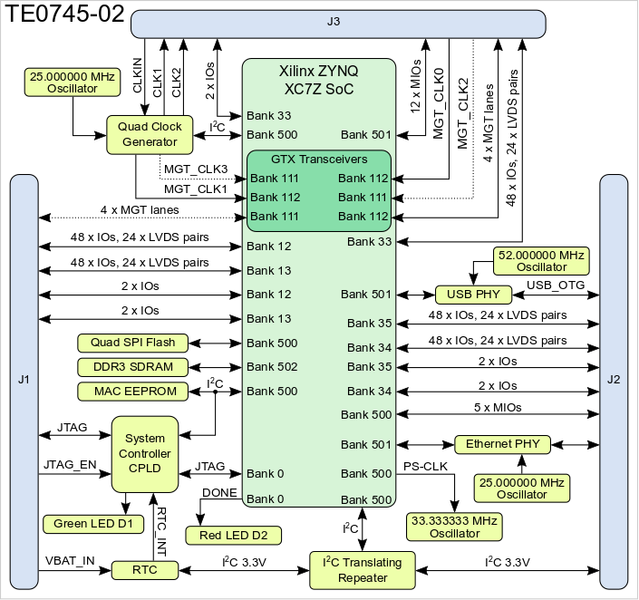
Figure 1: TE0745-02 Block Diagram
Main Components
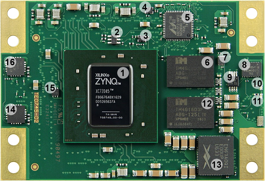
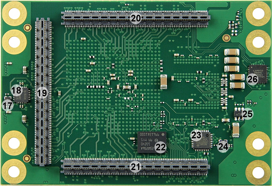
Figure 2: TE0745-02 SoC module
- Xilinx Zynq XC7Z family SoC, U1
- 256 Mbit Quad SPI Flash memory Micron N25Q256A, U12
- Reference clock signal oscillator SiTime SiT8008BI @33.333333 MHz, U12
- Reference clock signal oscillator SiTime SiT8008BI @25.000000 MHz, U9
- Marvell Alaska 88E1512 Gigabit Ethernet PHY, U3
- Intelligent Memory 512 MByte DDR3L-1600 SDRAM (8 Banks a 32 MWords, 16-bit word width), U3
- TI TPS51206 DDR3 memory termination regulator with buffered reference voltage VTTREF, U18
- Intersil ISL12020MIRZ Real-Time-Clock, U24
- TI TCA9517 level-shifting I2C bus repeater, U17
- Red LED, D2
- Green LED, D1
- Intelligent Memory 512 MByte DDR3L-1600 SDRAM (8 banks a 32 MWords, 16 Bit word width), U5
- Altera Enpirion EN63A0QI 12A DC-DC PowerSoC @1.0V (VCCINT), U4
- TI TPS74401RGW LDO DC-DC regulator @1.2V (MGTAVTT), U8
- TI TPS72018DRVR LDO DC-DC regulator @1.8V (MGTAUX), U6
- TI TPS74401RGW LDO DC-DC regulator @1.0V (MGTAVCC), U11
- Silicon Labs Si5338A I2C Programmable Quad Clock Generator, U13
- Reference clock signal oscillator SiTime SiT8008BI @25.000 MHz, U21
- Samtec ST5-80-1.50-L-D-P-TR 160-pin stacking strips (2 rows a 80 positions), J3
- Samtec ST5-80-1.50-L-D-P-TR 160-pin stacking strips (2 rows a 80 positions), J1
- Samtec ST5-80-1.50-L-D-P-TR 160-pin stacking strips (2 rows a 80 positions), J2
- 256 Mbit Quad SPI Flash memory (Micron N25Q256A, U14
- Microchip USB3320 USB transceiver PHY , U32
- Reference clock signal oscillator SiTime SiT8008BI @52.000000 MHz, U33
- Microchip 24AA025E48 EEPROM for MAC address, U23
- Lattice Semiconductor MachXO2-256HC System Controller CPLD, U2
Initial Delivery State
Storage Device Name | Content | Notes |
|---|---|---|
24AA025E48 EEPROM | User content not programmed | Valid MAC Address from manufacturer. |
SPI Flash OTP Area | Empty, not programmed | Except serial number programmed by flash vendor. |
SPI Flash Quad Enable bit | Programmed | - |
SPI Flash main array | Demo design | - |
eFUSE USER | Not programmed | - |
eFUSE Security | Not programmed | - |
| Si5338 OTP NVM | Default settings pre programmed | OTP not re-programmable after delivery from factory |
Table 1: Initial delivery state
Signals, Interfaces and Pins
Board to Board (B2B) I/O's
The B2B connectors are high-speed hermaphroditic stacking strips providing modular interface to the SoC's PL and PS I/Os. Both single ended and differential signalling LVDS pairs are supported.
| Bank | Type | B2B Connector | I/O Signals | LVDS Pairs | Bank Voltage | Notes |
|---|---|---|---|---|---|---|
| 12 | HR | J1 | 50 | 24 | VCCIO_12 pins J1-54, J1-55 | Voltage range 1.2V to 3.3V |
| 13 | HR | J1 | 50 | 24 | VCCIO_13 pins J1-112, J1-113 | Voltage range 1.2V to 3.3V |
| 33 | HP | J3 | 50 | 24 | VCCIO_33 pins J3-115, J3-120 | Voltage range 1.2V to 1.8V |
| 34 | HP | J2 | 50 | 24 | VCCIO_34 pins J2-29, J2-30 | Voltage range 1.2V to 1.8V |
| 35 | HP | J2 | 50 | 24 | VCCIO_35 pins J2-87, J2-88 | Voltage range 1.2V to 1.8V |
| 500 | MIO | J2 | 5 | - | 1.8V | - |
| 501 | MIO | J3 | 12 | - | 1.8V | - |
Table 2: Count, type and voltage range of SoC's PL and PS I/O banks pins available through B2B connectors.
For detailed information about the pin-out, please refer to the Pin-out Table.
MGT Lanes
The MGT bank signals of the SoC are routed to the B2B connectors J1 and J3. There are 8 high-speed bi-directional data lanes (Xilinx GTX transceivers) available composed as differential signaling pairs for both directions (RX/TX). On B2B connector J3 there are also clock input pins for MGT transceivers.
Following MGT lanes are available on the B2B connectors:
| Bank | Type | Lane Count | B2B Connector | Schematics Names / Connector Pins | MGT Bank's Reference Clock Inputs (LVDS pairs) |
|---|---|---|---|---|---|
| 111 | GTX | 4 | J1 | MGT_RX4_P, MGT_RX4_N, pins J1-23, J1-21 MGT_RX5_P, MGT_RX5_N, pins J1-17, J1-15 MGT_RX6_P, MGT_RX6_N, pins J1-11, J1-9 MGT_RX7_P, MGT_RX7_N, pins J1-3, J1-5 | Reference clock MGT_CLK3 from programmable Reference clock MGT_CLK2 from B2B connector |
| 112 | GTX | 4 | J3 | MGT_RX3_P, MGT_RX3_N, pins J3-68, J3-70 MGT_RX2_P, MGT_RX2_N, pins J3-62, J3-64 MGT_RX1_P, MGT_RX1_N, pins J3-56, J3-58 MGT_RX0_P, MGT_RX0_N, pins J3-50, J3-52 | Reference clock MGT_CLK1 from programmable Reference clock MGT_CLK0 from B2B connector |
Table 3: SoC's MGT lanes connections to the B2B connectors
JTAG Interface
JTAG access is provided through the SoC's PS configuration bank 0 and available on B2B connector J1.
| JTAG Signal | B2B Connector Pin |
|---|---|
| TCK | J1-143 |
| TDI | J1-142 |
| TDO | J1-145 |
| TMS | J1-144 |
Table 4: JTAG interface signals
| Note |
|---|
| JTAG_EN pin 148 in B2B connector J1 should be kept low or grounded for normal operation! |
System Controller I/O Pins
Following special purpose pins are connected to System Controller CPLD:
| Pin Name | Mode | Function | B2B Connector Pin | Default Configuration |
|---|---|---|---|---|
| JTAG_EN | Input | JTAG select | J1-148 | During normal operating mode the JTAG_EN pin should be in the low state and JTAG signals are forwarded to the Zynq SoC. |
| RST_IN_N | Input | Reset | J2-131 | Low-active Power-On reset pin, controls POR_B-signal (bank 500, pin C23) of Zynq chip. |
| PS_SRST | Input | Reset | J2-152 | Low-active PS system-reset pin of Zynq chip. |
| BOOTMODE | Output | Boot mode | J2-133 | Control line which sets in conjunction with signal 'BOOTMODE1' (B2B-pin J2-133) Permanent logic high in standard SC-CPLD firmware. |
| PWR_PL_OK | Input | Power good | J2-135 | Indicates stable state of PL supply voltage (low-active) after power-up sequence. |
| PWR_PS_OK | Input | Power good | J2-139 | Indicates stable state of PS supply voltage (low-active) after power-up sequence. |
| EN_PL | Output | Enable signal | - | Low active Enable-signal for activating PL supply voltage. Permanent logic high in standard SC-CPLD firmware. |
| MIO8 | Input | PS MIO | - | User I/O (pulled-up to PS_1.8V) |
| MIO0 | Input | PS MIO | J2-137 | User I/O |
| RTC_INT | Input | Interrupt signal | - | Interrupt-signal from on-board RTC |
| LED | Output | LED control | - | Green LED D1, indicates SC-CPLD activity by blinking |
Table 5: System Controller CPLD special purpose I/O pins
On-board LEDs
| LED | Color | Connected to | Description and Notes |
|---|---|---|---|
D1 | Green | System Controller CPLD, bank 3, pin 5 | System main status LED, blinking indicates system activity |
D2 | Red | Zynq chip (U1), bank 0 (config bank), 'DONE' (pin W9) | Reflects inverted DONE signal. ON when FPGA is not configured, OFF as soon as PL is configured. This LED remains OFF if System Controller CPLD can not power up the PL supply voltage. |
Table 6: LEDs of the module
Clocking
The SoC module has following reference clocking signals provided by external baseboard sources and on-board oscillators:
| Clock source | Schematic name | Frequency | Clock input destination |
|---|---|---|---|
| B2B connector J3, pins J3-74/J3-76 | CLKIN_N, CLKIN_P | User | Quad PLL clock generator U16, pin 1/2 |
| B2B connector J3, pins J3-75/J3-77 | MGT_CLK0_P, MGT_CLK0_N | User | MGT bank 112, pin R6/R5 |
| B2B connector J3, pins J3-81/J3-83 | MGT_CLK2_P, MGT_CLK2_N | User | MGT bank 111, pin W6/W5 |
| SiTime SiT8008BI oscillator, U21 | - | 25.000000 MHz | Quad PLL clock generator U16, pin 3 |
SiTime SiT8008BI oscillator, U12 | PS_CLK | 33.333333 MHz | Bank 500 (MIO0 bank), pin B24 |
| SiTime SiT8008BI oscillator, U23 | OTG-RCLK | 52.000000 MHz | USB 2.0 transceiver PHY U32, pin 26 |
| SiTime SiT8008BI oscillator, U9 | ETH_CLKIN | 25.000000 MHz | Gigabit Ethernet PHY U7, pin 34 |
Table 7: Clock sources overview
Default MIO Mapping
The configuration of the I/O's MIO12 - MIO15 and MIO40 - MIO51 are depending on the base-board peripherals connected to these pins.
| MIO | Function | Connected to | Notes | MIO | Function | Connected to | Notes | |
|---|---|---|---|---|---|---|---|---|
| 0 | GPIO | J2-137, SC CPLD bank 2, pin 14 | User configurable I/O on B2B. | 16..27 | ETH0 | Ethernet PHY U7 | RGMII | |
| 1 | QSPI0 | QSPI Flash Memory U14, pin C2 | SPI Flash-CS | 28..39 | USB0 | USB PHY U32 | ULPI | |
| 2 | QSPI0 | QSPI Flash Memory U14, pin D3 | SPI Flash-DQ0 | 40 | - | J2-150 | User configurable I/O on B2B. | |
| 3 | QSPI0 | QSPI Flash Memory U14, pin D2 | SPI Flash-DQ1 | 41 | - | J2-152 | User configurable I/O on B2B. | |
| 4 | QSPI0 | QSPI Flash Memory U14, pin C4 | SPI Flash-DQ2 | 42 | - | J2-154 | User configurable I/O on B2B. | |
| 5 | QSPI0 | QSPI Flash Memory U14, pin D4 | SPI Flash-DQ3 | 43 | - | J2-156 | User configurable I/O on B2B. | |
| 6 | QSPI0 | QSPI Flash Memory U14, pin B2 | SPI Flash-SCK | 44 | - | J2-158 | User configurable I/O on B2B. | |
| 7 | GPIO | USB PHY U32, pin 27 | Low active USB PHY Reset (pulled-up to PS_1.8V) | 45 | - | J2-160 | User configurable I/O on B2B. | |
| 8 | GPIO | SC CPLD bank 2, pin 13 | User I/O (pulled-up to PS_1.8V) | 46 | - | J2-145 | User configurable I/O on B2B. | |
| 9 | GPIO | Ethernet PHY U7, pin 16 | Ethernet PHY Reset | 47 | - | J2-147 | User configurable I/O on B2B. | |
| 10 | I²C | SCL line I2C-interface | 1.8V ref. voltage | 48 | - | J2-149 | User configurable I/O on B2B. | |
| 11 | I²C | SDA line I2C-interface | 1.8V ref. voltage | 49 | - | J2-151 | User configurable I/O on B2B. | |
| 12 | - | J2-123 | User configurable I/O on B2B. | 50 | - | J2-153 | User configurable I/O on B2B. | |
| 13 | - | J2-125 | User configurable I/O on B2B. | 51 | - | J2-155 | User configurable I/O on B2B. | |
| 14 | - | J2-127 | User configurable I/O on B2B. | 52 | ETH0 | USB PHY U32, pin 7 | MDC | |
| 15 | - | J2-129 | User configurable I/O on B2B. | 53 | ETH0 | USB PHY U32, pin 8 | MDIO |
Table 8: Default MIO Mapping
Gigabit Ethernet Interface
On-board Gigabit Ethernet PHY is provided with Marvell Alaska 88E1512 IC. The Ethernet PHY RGMII interface is connected to the Zynq Ethernet0 PS GEM0. I/O voltage is fixed at 1.8V for HSTL signalling. The reference clock input of the PHY is supplied from the on-board 25.000000 MHz oscillator (U9). The 125MHz PHY output clock (PHY_CLK125M) is routed to the B2B connector J2 pin 150.
| PHY Pin | ZYNQ PS | B2B | Notes |
|---|---|---|---|
| MDC/MDIO | MIO52, MIO53 | - | - |
| PHY LEDs | - | PHY_LED0: J2-144 | - |
| PHY_LED2 / INTn: | - | J2-148 | Active low interrupt line |
| PHY_CLK125M | - | J2-150 | 125 MHz Ethernet PHY clock out |
| CONFIG | - | - | Permanent high (PS_1.8V) |
| RESETn | MIO9 | - | Active low reset line |
| RGMII | MIO16..MIO27 | - | Reduced Gigabit Media Independent Interface |
| SGMII | - | - | Serial Gigabit Media Independent Interface |
| MDI | - | PHY_MDI0: J2-120 / J2-122 PHY_MDI1: J2-126 / J2-128 PHY_MDI2: J2-132 / J2-134 PHY_MDI3: J2-138 / J2-140 | Media Dependent Interface |
Table 9: Ethernet PHY interface connections
USB Interface
USB PHY is provided by USB3320 from Microchip. The ULPI interface is connected to the Zynq PS USB0. I/O voltage is fixed at 1.8V and PHY reference clock input is supplied from the on-board 25.000000 MHz oscillator (U15).
| PHY Pin | ZYNQ Pin | B2B Name | Notes |
|---|---|---|---|
| ULPI | MIO28..39 | - | Zynq USB0 MIO pins are connected to the PHY. |
| REFCLK | - | - | 52MHz from on board oscillator (U33). |
| REFSEL[0..2] | - | - | All pins set to GND selects the external reference clock frequency (52.000000 MHz). |
| RESETB | MIO7 | - | Active-low reset line. |
| CLKOUT | MIO36 | - | Set to high (1.8V VDDIO level) to select reference clock operation mode. |
| DP, DM | - | OTG_D_P, OTG_D_N, pin J2-149 / J2-151 | USB data lines. |
| CPEN | - | VBUS_V_EN, pin J2-141 | External USB power switch active-high enable signal. |
| VBUS | - | USB_VBUS, pin J2-145 | Connect to USB VBUS via a series of resistors, see reference schematics. |
| ID | - | OTG_ID, pin J2-143 | For an A-device connect to the ground. For a B-device, leave floating. |
Table 10: USB PHY interface connections
The schematics for the USB connector and required components is different depending on the USB usage. USB standard A or B connectors can be used for Host or Device modes. A Mini USB connector can be used for USB Device mode. A USB Micro connector can be used for Device mode, OTG Mode or Host Mode.
I2C Interface
The I2C interface on the B2B connector J2 pins 119 (I2C_33_SCL) and 121 (I2C_33_SDA) have PS_3.3V as a reference voltage.
Except the RTC (U24), all remaining I2C slave devices are operating with the reference voltage PS_1.8V via voltage level translating (3.3V ↔ 1.8V) I2C bus repeater (U17).
I2C addresses for on-board devices are listed in the table below:
| I2C Device | I2C Address | Notes |
|---|---|---|
| Zynq chip U1, bank 500 (PS MIO), pins MIO10 (SCL), MIO11 (SDA) | User programmable | Configured as I2C by default |
| Quad programmable PLL clock generator U16: pins 12 (SCL), 19 (SDA) | 0x70 | - |
| MAC Address EEPROM U23, pins 1 (SCL), 3 (SDA) | 0x53 | - |
| SC CPLD U2, bank 2, pins 16 (SDA), 17 (SCL) | User programmable | - |
| RTC, U24 | 0x6F | - |
| RTC RAM, U24 | 0x57 | - |
Table 11: Module's I2C-interfaces overview
Boot Process
TE0745 module supports different boot modes which are configurable by the control line 'BOOTMODE' and 'BOOTMODE_1'. The line 'BOOTMODE' is available on B2B connector pin J2-133, the line 'BOOTMODE_1' is connected to the System Controller CPLD on bank 1, pin 21.
The current boot mode will be set by the MIO pins MIO3...MIO5. The control line 'BOOTMODE' is connected to the 'MIO4' pin, 'BOOTMODE_1' to 'MIO5'.
Following table describes how to set the control lines to configure the desired boot mode:
| Boot Mode | MIO5 (BOOTMODE_1) | MIO4 (BOOTMODE) | MIO3 | Note |
|---|---|---|---|---|
JTAG | 0 | 0 | 0 | - |
| NOR | 0 | 0 | 1 | MIO3 pin is shared with QSPI Flash Memory (QSPI-DQ1) |
| NAND | 0 | 1 | 0 | - |
| QSPI Flash Memory | 1 | 0 | 0 | standard mode in current configuration |
| SD-Card | 1 | 1 | 0 | SD-Card on base board necessary |
Table 12: Selectable boot modes
On-board Peripherals
Flash
| Name | IC | ID | PS7 | MIO | Notes |
|---|---|---|---|---|---|
| SPI Flash | S25FL256SAGBHI20 | U14 | QSPI0 | MIO1..MIO6 | 32 MByte Flash memory at standard configuration |
MAC Address EEPROM
A Microchip 24AA025E48 serial EEPROM (U23) contains a globally unique 48-bit node address, which is compatible with EUI-48(TM) specification. The device is organized as two blocks of 128 x 8-bit memory. One of the blocks stores the 48-bit node address and is write protected, the other block is available for application use. It is accessible over I2C bus with slave device address 0x53.
RTC - Real Time Clock
An temperature compensated Intersil ISL12020M is used as Real Time Clock (U24). Battery voltage must be supplied to the clock from the base board via pin 'VBAT_IN' (J1-146). Battery backed registers can be accessed over I2C bus at slave address 0x6F. General purpose RAM of the RTC can be accessed at I2C slave address 0x57. RTC IC is supported by Linux so it can be used as hwclock device. The interrupt line 'RTC_INT' of the RTC is connected to System Controller CPLD bank 3 pin 4.
Programmable PLL Clock (Phase-Locked Loop)
There is a Silicon Labs I2C programmable quad PLL clock generator Si5338A (U16) on-board. It's output frequencies can be programmed by using the I2C-bus with address 0x70.
A 25 MHz (U21) oscillator is connected to pin 3 (IN3) and is used to generate the output clocks.
Once running, the frequency and other parameters can be changed by programming the device using the I2C-bus connected between the Zynq module (master) and reference clock signal generator (slave).
| Si5338A (U13) input | signal schematic name | Note |
|---|---|---|
IN1/IN2 | CLKIN_P, CLKIN_N | Reference clock signal from B2B connector J3, pin J3-74/J3-76 (base board decoupling capacitors and termination resistor necessary) |
IN3 | reference clock signal from oscillator SiTime SiT8008BI (U21) | 25.000000 MHz fixed frequency |
IN4/IN6 | pins put to GND | LSB (pin 'IN4') of the default I²C-adress 0x70 not activated |
IN5 | not connected | - |
| Si5338A (U13) output | signal schematic name | Note |
CLK0 A/B | MGTCLK1_P, MGTCLK1_N | reference clock signal to MGT bank 112, pin U6/U5 (100 nF decoupling capacitors) |
CLK1 A/B | CLK1_P, CLK1_N | clock signal routed to B2B connector, pin J3-80/J3-82 |
CLK2 A/B | CLK2_P, CLK2_N | clock signal routed to B2B connector, pin J3-86/J3-88 |
| CLK3 A/B | MGTCLK3_P, MGTCLK3_N | reference clock signal to MGT bank 111, pin AA6/AA5 (100 nF decoupling capacitors) |
Table 13: Pin description of PLL clock generator Si5338A
Power and Power-On Sequence
Power Supply
Power supply with minimum current capability of 3A for system startup is recommended.
Power Consumption
| Power Input Pin | Typical Current |
|---|---|
| PL_VIN | TBD* |
| PS_VIN | TBD* |
| PS_3.3V | TBD* |
Table 14: Maximum current of power supplies. *to be determined soon with reference design setup.
For the lowest power consumption and highest efficiency of on board DC-DC regulators it is recommended to powering the module from one single 3.3V supply. All input power supplies have a nominal value of 3.3V. Although the input power supplies can be powered up in any order, it is recommended to power them up simultaneously.
Power-On Sequence
The on-board voltages of the TE0745 SoC module will be powered-up in order of a determined sequence after the external voltages 'PL_VIN', 'PS_VIN' and 'PS_3.3V' are available.
| Warning |
|---|
| To avoid any damage to the SoC module, check for stabilized on-board voltages in steady state before powering up the SoC's I/O bank voltages VCCO_x. |
Core voltages and main supply voltages have to reach stable state and their "Power Good"-signals have to be asserted before other voltages like PL bank's I/O voltages can be powered up.
It is important that all baseboard I/Os are 3-stated at power-on until the "Power Good"-signals 'PWR_PS_OK' (J2-139) and 'PWR_PL_OK' (J2-135) are high, meaning that all on-module voltages have become stable and module is properly powered up.
Following diagram clarifies the sequence of enabling the particular on-board voltages:
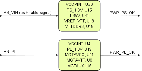
Figure 3: Power-up sequence diagram
See Xilinx datasheet DS191 for additional information. User should also check related base board documentation when intending base board design for TE0745 module.
Power Rails
Voltages on B2B | B2B J1 Pin | B2B J2 Pin | B2B J3 Pin | Input/ | Note |
|---|---|---|---|---|---|
| PL_VIN | 147, 149, 151, 153, | - | - | Input | supply voltage |
| PS_VIN | - | 154, 156, 158 | - | Input | supply voltage |
| PS_3.3V | - | 160 | - | Input | supply voltage |
| VCCIO12 | 54, 55 | - | - | Input | high range bank I/O voltage |
| VCCIO13 | 112, 113 | - | - | Input | high range bank I/O voltage |
| VCCIO33 | - | - | 115, 120 | Input | high performance bank I/O voltage |
| VCCIO34 | 29, 30 | - | Input | high performance bank I/O voltage | |
| VCCIO35 | 87, 88 | - | Input | high performance bank I/O voltage | |
| VBAT_IN | 146 | - | - | Input | RTC (battery-backed) supply voltage |
| PS_1.8V | - | 130 | - | Output | internal 1.8V voltage level (Process System supply) |
Table 15: Power rails of the SoC module on accessible connectors
Bank Voltages
Bank | Schematic Name | Voltage | Voltage Range |
|---|---|---|---|
| 0 (config) | VCCIO_0 | PL_1.8V if R67 is equipped | - |
| 500 (MIO0) | PS_1.8V | 1.8V | - |
| 501 (MIO1) | PS_1.8V | 1.8V | - |
| 502 (DDR3) | 1.35V | 1.35V | - |
| 12 HR | VCCIO_12 | User | HR: 1.2V to 3.3V |
| 13 HR | VCCIO_13 | User | HR: 1.2V to 3.3V |
| 33 HP | VCCIO_33 | User | HP: 1.2V to 1.8V |
| 34 HP | VCCIO_34 | User | HP: 1.2V to 1.8V |
| 35 HP | VCCIO_35 | User | HP: 1.2V to 1.8V |
Table 16: Range of SoC module's bank voltages
B2B connectors
| Include Page | ||||
|---|---|---|---|---|
|
Variants Currently In Production
| Module Variant | Zynq SoC | SoC Junction Temperature | Operating Temperature Range |
|---|---|---|---|
| TE0745-02-30-1I | XC7Z030-1FBG676I | –40°C to +100°C | Industrial |
| TE0745-02-35-1C | XC7Z035-1FBG676C | 0°C to +85°C | Commercial |
| TE0745-02-45-1C | XC7Z045-1FBG676C | 0°C to +85°C | Commercial |
| TE0745-02-45-2I | XC7Z045-2FBG676I | –40°C to +100°C | Industrial |
Table 17: Differences between variants of Module TE0808-04
Technical Specification
Absolute Maximum Ratings
Parameter | Min | Max | Units | Notes |
|---|---|---|---|---|
| PL_VIN | -0.3 | 5 | V | TI TPS720 data sheet |
| PS_VIN | -0.3 | 7 | V | TI TPS82085 data sheet |
| PS_3.3V | 3.135 | 3.465 | V | 3.3V nominal ± 5% Attention: PS_3.3V is directly connected to numerous |
| VBAT supply voltage | -1 | 6.0 | V | ISL12020MIRZ data sheet |
| PL IO bank supply voltage for HR I/O banks (VCCO) | -0.5 | 3.6 | V | - |
PL IO bank supply voltage for HP | -0.5 | 2.0 | V | - |
| I/O input voltage for HR I/O banks | -0.4 | VCCO_X+0.55 | V | - |
| I/O input voltage for HP I/O banks | -0.55 | VCCO_X+0.55 | V | - |
| GT receiver (RXP/RXN) and transmitter (TXP/TXN) | -0.5 | 1.26 | V | - |
Voltage on module JTAG pins | -0.3 | 3.6 | V | MachX02 Family data sheet |
Storage temperature | -40 | +85 | °C | Limits of ISL12020MIRZ RTC chp. |
| Storage temperature without the ISL12020MIRZ | -55 | +100 | °C | Limits of DDR3 memory chips. |
| Note |
|---|
| Assembly variants for higher storage temperature range are available on request. |
Recommended Operating Conditions
| Parameter | Min | Max | Units | Notes | Reference Document |
|---|---|---|---|---|---|
| PL_VIN | 3.3 | 4.5 | V | - | TI TPS720 data sheet |
| PS_VIN | 3.3 | 6.0 | V | - | TI TPS82085 data sheet |
| PS_3.3V | 3.135 | 3.465 | V | - | 3.3V nominal ± 5% |
| VBAT_IN supply voltage | 2.7 | 5.5 | V | - | ISL12020MIRZ data sheet |
PL I/O bank supply voltage for HR | 1.14 | 3.465 | V | - | Xilinx datasheet DS191 |
PL I/O bank supply voltage for HP | 1.14 | 1.89 | V | - | Xilinx datasheet DS191 |
| I/O input voltage for HR I/O banks | -0.20 | VCCO_X+0.20 | V | - | Xilinx datasheet DS191 |
| I/O input voltage for HP I/O banks | -0.20 | VCCO_X+0.20 | V | - | Xilinx datasheet DS191 |
| GT receiver (RXP/RXN) and transmitter (TXP/TXN) | (*) | (*) | V | (*) Check datasheet | Xilinx datasheet DS191 |
| Voltage on Module JTAG pins | 3.135 | 3.6 | V | JTAG signals forwarded to Zynq module config bank 0 | MachX02 Family Data Sheet |
Operating Temperature Ranges
Commercial grade: 0°C to +70°C.
Industrial grade: -40°C to +85°C.
Module operating temperature range depends also on customer design and cooling solution. Please contact us for options.
| Note |
|---|
| Please check Xilinx datasheet DS191 (for XC7Z030) for complete list of absolute maximum and recommended operating ratings. |
Physical Dimensions
Module size: 52 mm × 76 mm. Please download the assembly diagram for exact numbers
Mating height with standard connectors: 4mm
PCB thickness: 1.6mm
Highest part on PCB: approx. 3mm. Please download the step model for exact numbers
All dimensions are given in millimeters.
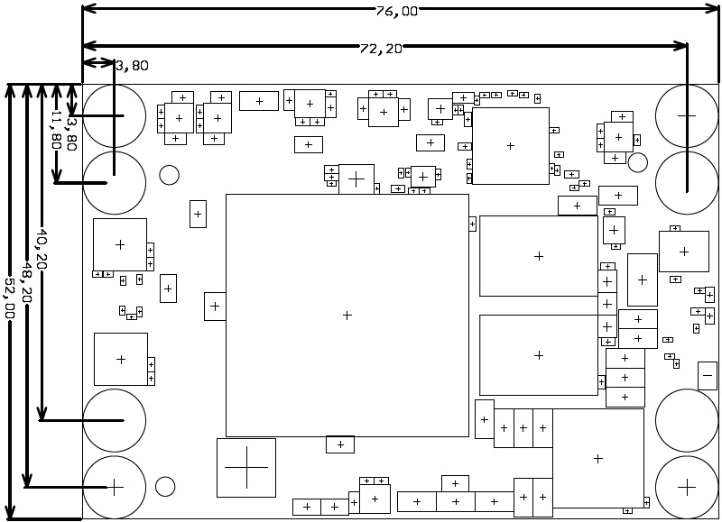
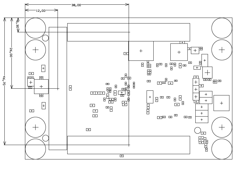
Figure 4: Physical dimensions of the TE0745 SoC module
Weight
24 g - Plain module
Revision History
Hardware Revision History
| Date | Revision | Notes | Link to PCN | Documentation Link |
|---|---|---|---|---|
| 2016-10-11 | 02 | Production release | TE0745-02 | |
| 2016-04-18 | 01 | Prototypes | TE0745-01 |
Hardware revision number is written on the PCB board together with the module model number separated by the dash.
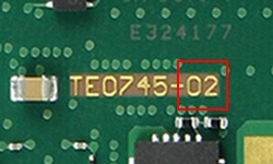
Figure 5: TE0745 module revision number
Document Change History
| Date | Revision | Contributors | Description |
|---|---|---|---|
| 2017-03-31 | Ali Naseri, Jan Kumann | First TRM release. | |
| 2017-02-05 | V1
| Jan Kumann | Initial document. |
Disclaimer
| Include Page | ||||
|---|---|---|---|---|
|
Overview
Content Tools