Page History
...
The Trenz Electronic TE0706 carrier board provides functionality for testing, evaluation and development purposes of company's 4 x 5 cm SoMs (System on Module). The Carrier Board carrier board is equipped with various components and connectors for different configuration setups and needs. The interfaces of the SoM's functional components and multipurpose I/Os of the SoM's PL logic are connected via board-to-board connectors to the Carrier Boardcarrier board's components and connectors for easy user access.
See "4 x 5 cm carriers" page for more information about supported 4 x 5 cm SoMs.
Key Features
- 3 x Samtec LSHM Series Board to Board Connectors
- VG96 VG96 backplane connector (mounting holes and solder pads, J6) and 50-pin IDC male connector socket (J5) to access FPGA bank's for access to PL IO-bank pins
- SDIO port expander with voltage-level translation
- Micro SD card socket, routed to B2B-connector JB1USB type A
- USB 2.0 type A connector, optionally Micro USB 2.0 connector (OTG-mode) connector (OTG mode), routed to B2B-connecor JB3
- 1 x user-push button S2, routed to RESIN-pin on B2B-connector JB2. By default it is by default configured as system reset button.
- 1 x RJ45 Gigabit Ethernet MagJack J3, PHY_connected via MDI interface routed to B2B - connector JB1.
- 1 x Marvell Alaska 88E1512 Ethernet PHY, routed to B2B-connector JB3 and accessible via providing Ethernet interface with RJ45 Gigabit Ethernet MagJack J2
- Barrel jack for 5 V Power Supply input5V power supply barrel jack
- 4 A High-Efficiency Power SoC DC-DC Step-Down Converter (Enpirion EN6347) for 3.3 V Power Supply
- Trenz 4 x 5 Module Socket (3 x Samtec LSHM series connectors)
- 3V power supply
- JTAG- JTAG / UART-pins on interface (12-pin header JX1, routed to B2B-connector JB2)
- DIP-user configurable DIP switch S1 to set System Controller CPLD signals on SoM
- 3 x x VCCIO selection jumper J10, J11 and J12 to set SoM's bank voltages
Block Diagram
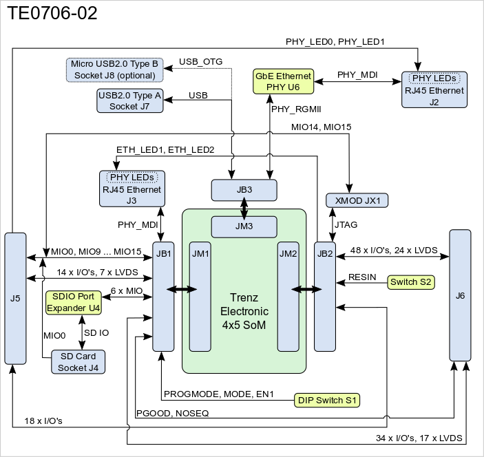
Figure 1: TE0706-02 Block Diagram
Main Components
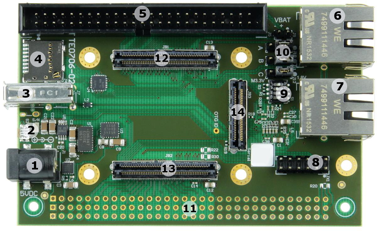
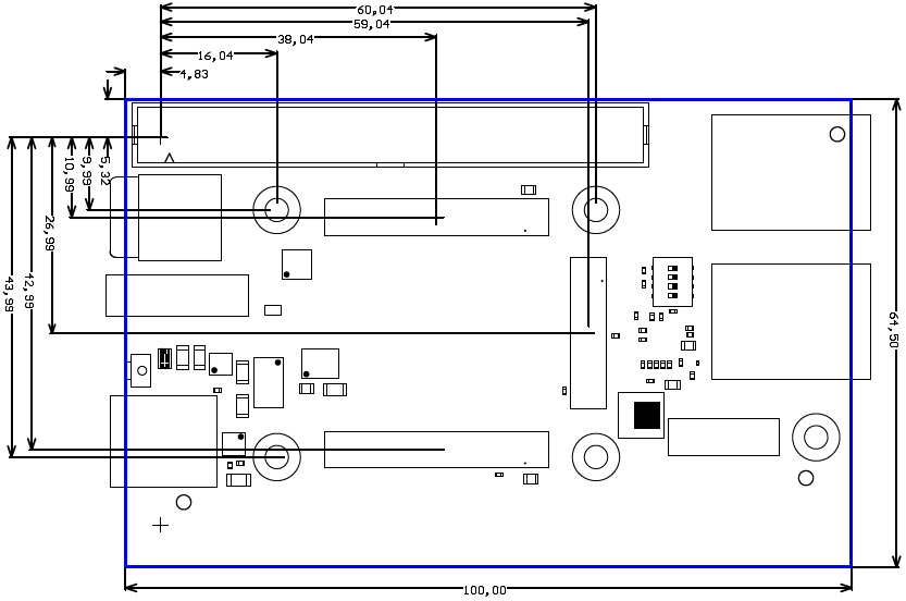
Figure 2: TE0706-02 Carrier Board
- 5V power connector jack, J1
- Reset switch, S2
- USB type A receptacle, J7
- Micro SD card socket with Card Detect, J4
- 50 pin IDC male connector, J5
- 1000Base-T Gigabit RJ45 Ethernet MagJack, J3
- 1000Base-T Gigabit RJ45 Ethernet MagJack, J2
- JTAG- / UART-connector, JX1
- User DIP-switch block, S1
- VCCIO voltage selection jumper block, J10 - J12
- External connector (VG96) placeholder, J6
- Samtec Razor Beam™ LSHM-150 B2B connector, JB1
- Samtec Razor Beam™ LSHM-150 B2B connector, JB2
- Samtec Razor Beam™ LSHM-130 B2B connector, JB3
Initial Delivery State
...
- VCCIO voltage selection jumpers are all set to 1.8 V.
- S2 switch configured as reset button.
- One VG96 backplane connector is not soldered to the board, but is included in the package as separate component.
...
This header has a 'XMOD FTDI JTAG Adapter'-compatible pin-assignment, so the XMOD-FT2232H adapter-board TE0790 can be used in conjunction with the TE0706 Carrier Board carrier board to program the mounted SoM via USB interface.
| JX1 pinConfigured | asPin Schematic Name | B2B |
|---|---|---|
| C (pin 4) | TCK | JB2-100 |
| D (pin 8) | TDO | JB2-98 |
| F (pin 10) | TDI | JB2-96 |
| H (pin 12) | TMS | JB2-94 |
| A (pin 3) | MIO15 | JB1-86 (usable configurable as UART RX- / TX-line) |
| B (pin 7) | MIO14 | JB1-91 (usable configurable as UART RX- / TX-line) |
Table 1: JTAG- / UART-header JX1 pin-assignment
Micro SD Card Socket
Micro SD Card socket is not directly wired to the B2B connector pins, but routed through a Texas Instruments TXS02612 SDIO port expander, which is needed for voltage translation due to the different voltage levels of the Micro SD Card and MIO bank 501 of the Xilinx Zynq 7000 chip. The Micro SD Card has 3.3 V signal voltage-level, but the MIO Bank 501 on the Xilinx Zynq 7000 chip is set to 1.8 V.
...
| PHY | B2B-pin | Notes |
|---|---|---|
| MDC/MDIO | JB3-49, JB3-51 | - |
| LED0 | - | Connected to Ethernet jack J2 LED0 (green). |
| LED1 | - | Connected to Ethernet jack J2 LED1 (green). |
| INT | JB3-33 | - |
| CONFIG | JB3-60 | - |
| RESET | JB3-53 | - |
| RGMII | JB3-37 - JB-44, JB3-47, JB3-57 - JB-59 | Reduced Gigabit Media Independent Interface. 12 pins. |
| SGMII | - | Serial Gigabit Media Independent Interface. Not connected. |
| MDI | - | Media Dependent Interface. Connected to Gigabit Ethernet MagJack J2. |
Table 2: Ethernet PHY interface connections
RJ45 Gigabit Ethernet MagJack J3
...
There is also the option to equip a micro Micro USB 2.0 type B receptacle socket (J8) to the board as alternative.
| Info |
|---|
| Note: Pin OTG-ID is only assigned to USB 2.0 type B socket. |
DIP-Switch S1
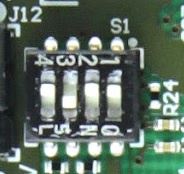
Figure 2: User DIP Switch S1
| Switch | Signal Name | ON | OFF | Notes |
|---|---|---|---|---|
| S1-1 | - | - | - | Not connected. |
| S1-2 | PROGMODE | JTAG enabled for programing mounted SoM's Zynq-SoC. | JTAG enabled for programing mounted SoM's SC-CPLD. | - |
| S1-3 | MODE | Drive SoM SC CPLD pin 'MODE' low. | Leave SoM SC CPLD pin 'MODE' open. | Boot mode configuration, if supported by SoM. (Depends also on SoM's SC-CPLD firmware). |
| S1-4 | EN1 | Drive SoM SC CPLD pin 'EN1' low. | Drive SoM SC CPLD pin 'EN1' high. | Usually used to enable/disable FPGA core-voltage supply. (Depends also on SoM's SC CPLD firmware). Note: Power-on sequence will be intermitted if S1-4 is set to OFF and if functionality is supported by SoM. |
Table 3: Functionality of the states of DIP-switch S1
Connector J5 and J6
On the TE0706-02 carrier board there is one 50-pin IDC male connector socket J5 and a place-holder (VG96-Connector solder pads) J6 to provides access to SoM's PL IO-bank-pins. With this user interfaces, a large quantity of IO's are also usable as LVDS-pairs and different VCCIO's are available to operate the IO's properly.
...
| Connector Designator | Connector Type | Count of IO's | Count of LVDS Pairs | Available VCCIO's | InterfacesAvailable Control Lines and Signals |
|---|---|---|---|---|---|
| J5 | 50-pin IDC male | 40 | 16 | 3.3V, | access to the LEDs of MagJack J2 , access to the MIO0-bank MIO0,MIO9...MIO15 of the Zynq module |
| J6 | VG96-Connector | 82 | 41 | 3.3V, | PGOOD-, NOSEQ-Signal of SC-CPLD of mounted 4 x 5 SoM |
Table 4: Pin-assignment of connector J5 and J6
Power and Power-On Sequence
...
It is not allowed to feed any voltage to any external I/O pin before there is no power indication on M3.3VOUT pins. Presence of 3.3V on B2B JB2 connector pins 9 and 11 indicates that module is properly powered up and ready. The 1.8V voltage-level on base-board for supplying PL I/O bank supply-voltages will be powered up after the module's 3.3V voltage-level has reached stable state and M3.3VOUT is available on the B2B-connector JB2, pins 9 and 11.
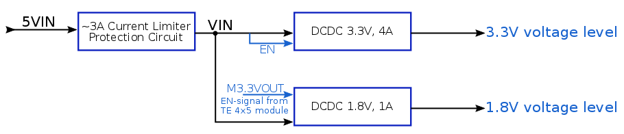
If VCCIOA or VCCIOC will be powered through the dedicated pins of external connector J6, then corresponding VCCIO jumpers J10 and J12 should be removedFigure 3: TE0706-02 power-up sequence diagram.
Base-board supply-voltage configuration
...
| Note |
|---|
Note: The corresponding PL I/O bank supply-voltages of the 4 x 5 SoM to the selectable base-board voltages VCCIOA, VCCIOB and VCCIOC are depending on the mounted 4 x 5 SoM and varying in order of the used model. Refer to the SoM's schematic for information about the specific pin assignments on module's B2B-connectors regarding the PL I/O bank supply-voltages and to the 4 x 5 Module integration Guide for VCCIO voltage options. |
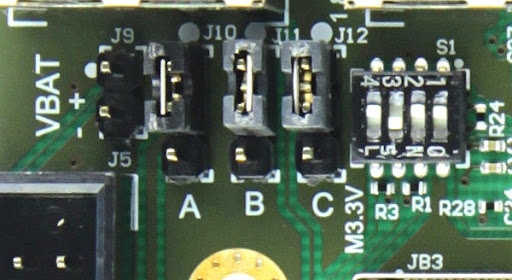
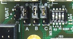
Figure 4: Base-board supply-voltages (VCCIOA, VCCIOB, VCCIOC) selection-jumpers.
Following table shows how to configure the voltage-levels of base-board supply-voltages VCCIOA, VCCIOB and VCCIOC by jumper, 0-Ohm-resistor or by feeding the supply voltage through connector J6:
| Supply Voltage by Jumper | Supply Voltage by 0-Ohm Resistor | Supply Voltage by Connector J6 | ||||
|---|---|---|---|---|---|---|
| Voltage Level | 1.8V | 3.3V | 1.8V | 3.3V | Variable | |
| VCCIOA | J10: 1-2, 3 | J10: 1, 2-3 | - | R20 | J6 pin B32 | |
| VCCIOB | J11: 1-2, 3 | J11: 1, 2-3 | R29 | R21 | - | |
| VCCIOC | J12: 1-2, 3 | J12: 1, 2-3 | R30 | R22 | J6 pin B1 | |
Table 5: Configuration of baseboard supply-voltages. Jumper-Notification: 'Jx: 1-2, 3' means pins 1 and 2 are connected, 3 is open. 'Jx: 1, 2-3' means pins 2 and 3 are connected, 1 is open.
Only one supply-source is allowed to configure the base-board supply-voltages, either by jumper, by 0-Ohm-resistor or by connector J6. If a supply-voltage is configured by 0-Ohm-resistor or connector J6, then the corresponding configuration-jumper has to be removed. There aren't 0-Ohm-resistors and supply-voltages by connector J6 allowed if the corresponding base-board supply-voltage is configured by jumper. Vice versa jumpers and 0-Ohm-resistors have to be removed if supplying corresponding base-board supply-voltage by connector J6.
Note: If supplying base-board supply-voltages by connector J6, the module's internal 3.3V voltage-level on pins 9 and 11 of B2B-connector JB2 has to be reached stable state.
...
All dimensions are given in millimeters.
Operating Temperature Ranges
...
| Date | Revision | Notes | PCN | Documents |
|---|---|---|---|---|
| 2016-06-28 | 02 | First production revision | - | |
- | 01 | Prototypes | - |
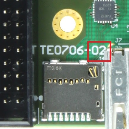

Hardware revision number is printed on the PCB board next to the module model number separated by the dash.
...
Overview
Content Tools