Page History
...
Table 9: Pin description of PLL clock generator Si5338A
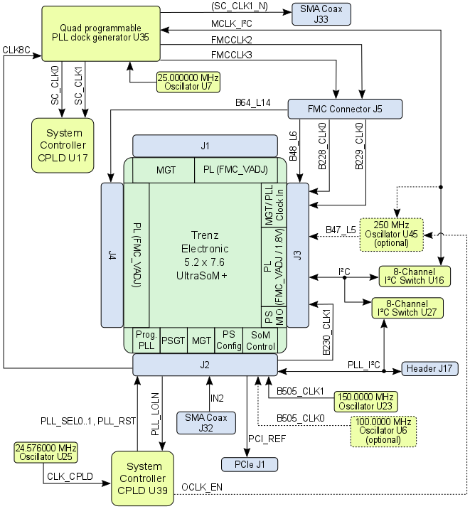
Figure 89: Clocking Configuration of TE0808 SoM on TEBF0808 Carrier Board
...
Table 7: Ethernet PHY interface connections
8-Channel I²C Switches
The I2C interface on B2B connector J2 pins 119 (I2C_33_SCL) and 121 (I2C_33_SDA) have PS_3.3V as reference voltage.
...
Power and Power-On Sequence
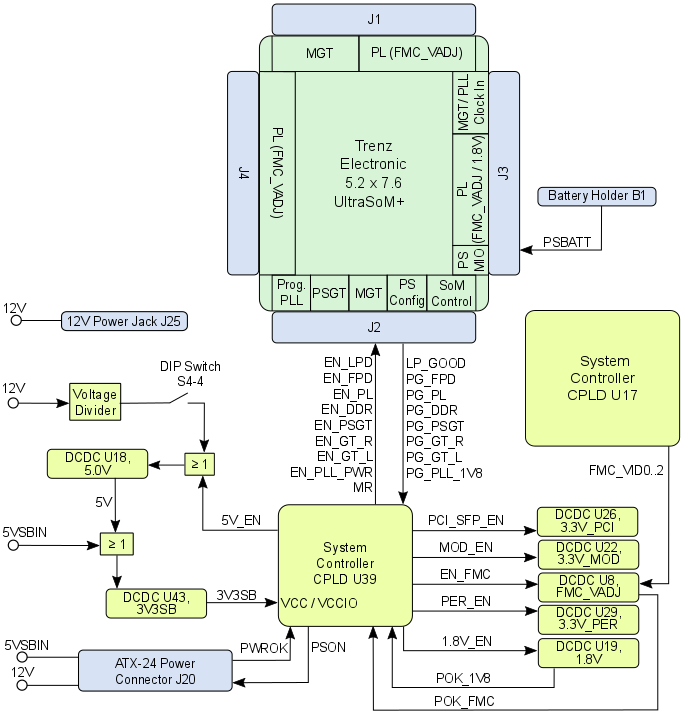
Figure 10: TEBF0808 Power-Management
Power Consumption
The maximum power consumption of a module mainly depends on the design which is running on the FPGA.
...
There are following dependencies how the initial voltages of the power rails on the B2B connectors are distributed to the on-board DCDC converters, which power up further DCDC converters and the particular on-board voltages:
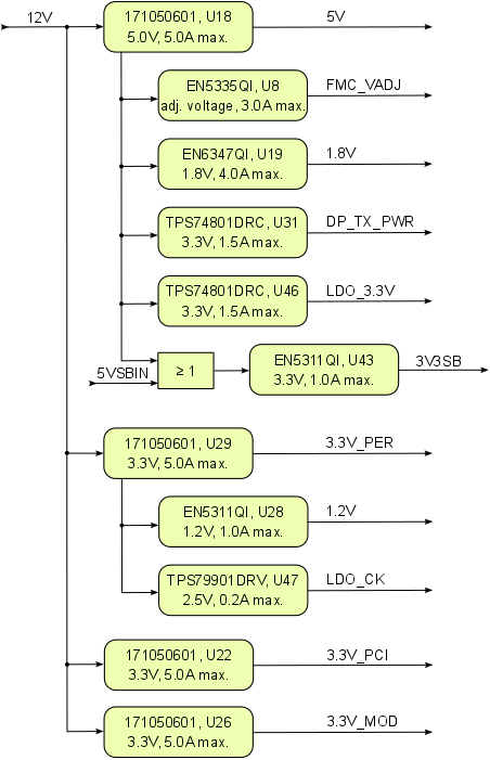
Figure 311: Power Distribution Diagram
...
Following diagram clarifies the sequence of enabling the three power instances utilizing the DCDC converter control signals ('Enable', 'Power-Good'), which will power-up in descending order as listed in the blocks of the diagram.
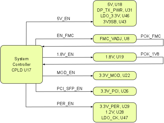
Figure 412: Power-On Sequence Utilizing DCDC Converter Control Signals
...
Overview
Content Tools