Page History
| HTML |
|---|
<!--
Template Revision 1.6
(HTML comments will be not displayed in the document, no need to remove them. For Template/Skeleton changes, increase Template Revision number. So we can check faster, if the TRM style is up to date).
--> |
| Scroll Ignore |
|---|
Download PDF version of this document. |
...
System Controller CPLD
The system controller System Controller CPLD is used to coordinate the configuration of the FPGA. The FPGA is held in reset (by driving the PROG_B signal) until the power supplies have sequenced. Setting input signal RESIN low will also reset the FPGA. This signal can be driven from the user’s PCB via the board connector.
It is possible for the user to create their own system controller User can create its own System Controller CPLD design using the Lattice Diamond software . Once created the design can be programmed and program it into the device using the JTAG pinsinterface. The JTAGMODE signal JTAGMODE should be set to 3.3V to enable programming mode. For , for normal module operation it should be set to 0V.
The LED that is Green LED D4 (C_LED) connected to the system controller flashes System Controller CPLD is to indicate the state status of the boardmodule.
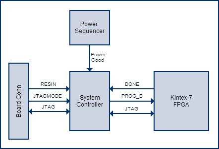
Figure 5: System Controller block diagram.
...
Power Consumption
| Power Input Pin | Max Typical Current |
|---|---|
| VIN | TBD* |
| 3.3VIN | TBD* |
Table 8: Maximum current of power supplies.
* TBD - To Be Determined soon with reference design setup.
Lowest power consumption is achieved when powering the module from single 3.3V supply. When using split 3.3V/5V power supplies, the power consumption (and heat dissipation) will rise, this is due to the DC/-DC converter efficiency (it decreases when VIN/VOUT ratio rises).
...
Voltages on B2B-Connectors | B2B JM1 Pin | B2B JM2 Pin | B2B Direction | Note |
|---|---|---|---|---|
| VIN | 1, 3, 5 | 2, 4, 6, 8 | Input | Supply voltage. |
| 3.3VIN | 13, 15 | - | Input | Supply voltage. |
| VCCIO12 | - | 7, 9 | Input | High range bank voltage. |
| VCCIO13 | 9, 11 | - | Input | High range bank voltage. |
| VCCIO15 | - | 5 | Input | High range bank voltage. |
| VCCIO16 | - | 1, 3 | Input | High range bank voltage. |
| 3.3V | - | 10, 12, 91 | Output | Internal 3.3V voltage level. |
...
Variants Currently In Production
Module Variant | FPGA | U15 | FPGA Junction Temperature |
|---|
| Temperature |
|---|
| Grade | |||
|---|---|---|---|
| TE0741-03-070-2CF | XC7K70T-2FBG676C | - | 0°C to 85°C |
| Commercial grade | |||
| TE0741-03-070-2IF | XC7K70T-2FBG676I | - | -40°C to 100°C |
|---|
| Industrial grade | |||
| TE0741-03-160-2CF | XC7K160T-2FBG676C | - | 0°C to 85°C |
|---|
| Commercial grade | |||
| TE0741-03-160-2C1 | XC7K160T-2FFG676C | - | 0°C to 85°C |
|---|
| Commercial grade | |||
| TE0741-03-160-2IF | XC7K160T-2FBG676I | - | -40°C to 100°C |
|---|
| Industrial grade | |||
| TE0741-03-325-2CF | XC7K325T-2FBG676C | EN63A0QI | 0°C to 85°C |
|---|
| Commercial grade | |||
| TE0741-03-325-2IF | XC7K325T-2FBG676I | EN63A0QI | -40°C to 100°C |
|---|
| Industrial grade | |||
| TE0741-03-410-2CF | XC7K325T-2FBG676C | EN63A0QI | 0°C to 85°C |
|---|
| Commercial grade |
Table 11: Module TE0741-03 variants.
...
| Date | Revision | Contributors | Description | ||||||||
|---|---|---|---|---|---|---|---|---|---|---|---|
| Jan Kumann | Few improvements. Template revision added. | |||||||||
| 2017-07-20 | v.57 | John Hartfiel | Correction: PLL default output CLKs. | ||||||||
| 2017-06-07 | v.55 | Jan Kumann | Minor formatting | ||||||||
| 2017-06-02 | v.50 | Jan Kumann | REV03 specific update. | ||||||||
| 2017-01-22 | v.42 | Jan Kumann | New block diagram added. | ||||||||
| 2017-01-13 | v.38 | Jan Kumann | New product images and physical dimension drawings. Formatting improvements and small corrections. | ||||||||
| 2017-01-12 | v.21 | John Hartfiel | Correction: B2B and FPGA bank location. | ||||||||
| 2016-12-14 | v.19 | Ali Naseri | TRM revision. | ||||||||
| 2013-12-02 | v.1 | Antti Lukats, Jon Bean | Initial version. |
...
Overview
Content Tools