Page History
| HTML |
|---|
<!--
Template Revision 1.64
(HTML comments will be not displayed in the document, no need to remove them. For Template/Skeleton changes, increase Template Revision number. So we can check faster, if the TRM style is up to date).
--> |
| HTML |
|---|
<!--
General Notes:
If some section is CPLD firmware dependent, make a note and if available link to the CPLD firmware description. It's in the TE shop download area in the corresponding module -> revision -> firmware folder.
--> |
| HTML |
|---|
<!--
General Notes:
Designate all graphics and pictures with a number and a description. For example "Figure 1: TE07xx-xx Block Diagram" or "Table 1: Initial delivery state". "Figure x" and "Table x" have to be formatted to bold.
--> |
| Scroll Ignore |
|---|
Download PDF version of this document. |
| Scroll pdf ignore | |
|---|---|
Table of Contents
|
Overview
| Scroll Only (inline) |
|---|
Refer to https://shop.trenz-electronic.de/de/Download/?path=Trenz_Electronic/XMOD/TE0791 for downloadable version of this manual and additional technical documentation of the product.
|
The Trenz Electronic TE0791-01 is an adapter board for use with the XMOD TE0790 board. The adapter board provides several connector types to get access to the signals and interfaces of the XMOD board. As further option footprints are available for JST Wire-To-Board IDC connectors with two different pin-assignments.
Key Features
- Xmod form-factor
- size: 20 x 25 mm
- M3 mounting hole
- Different connector types available
- 2x6 PMOD connector
- JTAG 1-row pin header female
- 2x optional JST Wire-To-Board 6-pin IDC connector
- 2x optional JST Wire-To-Board 10-pin IDC connector
- IDC connectors with different pin-assignment each
Block Diagram
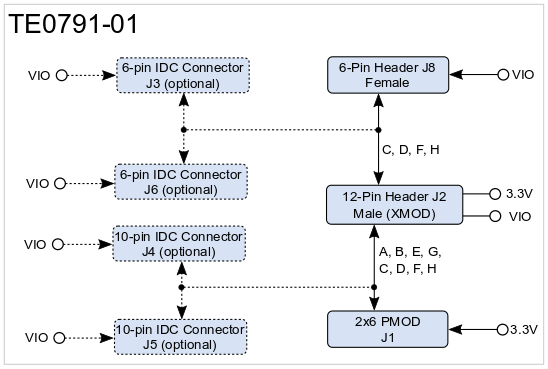
Figure 1: TE0790-02 block diagram.
Main Components
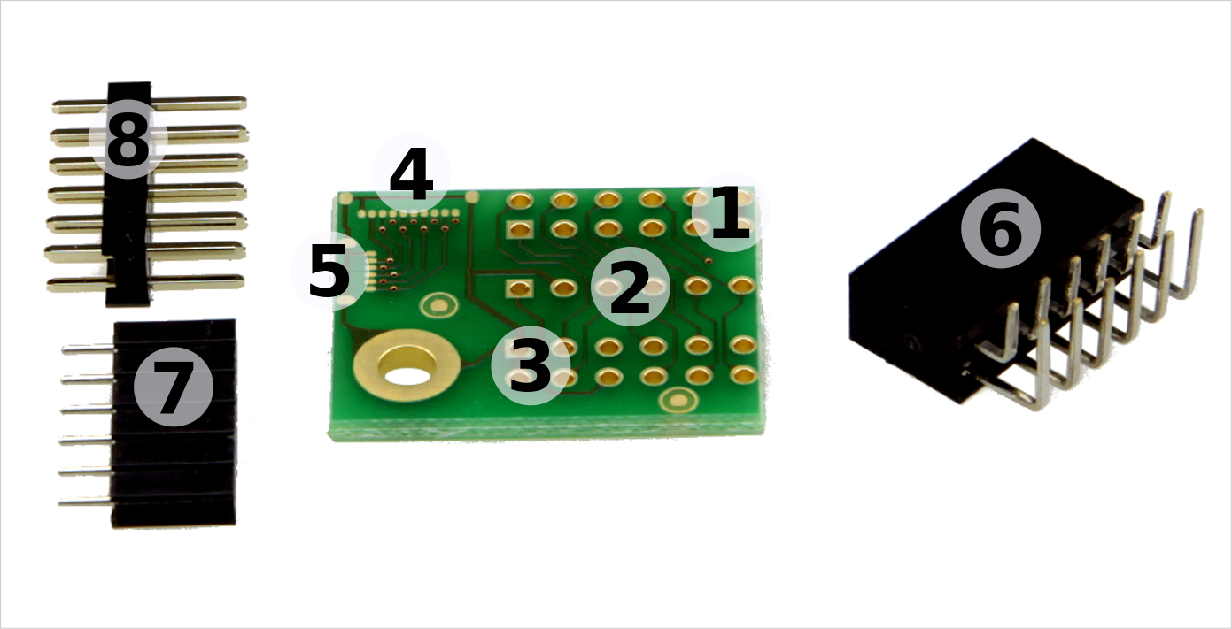
Figure 2: TE0790-02 main components. Bottom side view
- 2x6 PMOD connector solder pads, J1 (on top side)
- 6-Pin header solder pads, J8
- 12-Pin header solder pads, J2
- 10-pin IDC connector solder pads, J4 (solder pads J5 on top side)
- 6-pin IDC connector solder pads, J3 (solder pads J6 on top side)
- 2x6 PMOD connector
- 1-row 6-pin header female (2.54 mm pitch)
- 2-row 12-pin header male (2.54 mm pitch)
Signals, Interfaces and Pins
2x6 Pin Header
The 2x6 pin header (2.54mm grid size, male) J2 have to be connected to the corresponding XMOD pin header on the TE0790 adapter board. The signal assignment of the pin header on the TE0790 adapter board depends on the configuration its System Controller CPLD firmware.
The pin assignment on the adapter board is the same as on the TE0790 XMOD board:
| Signal | J2 Pin Name | J2 Pin Name | Signal |
|---|---|---|---|
| GND | 1* | GND | |
| User Defined | C | A | User Defined |
| VIO | VDD 3.3V | ||
| User Defined | D | B | User Defined |
| User Defined | F | E | User Defined |
| User Defined | H | G | User Defined / Button (Reset_n) |
Table 1: Pin header J2 signal assignment. *pin 1 on header J2 of the adapter board
1x6 Pin Header
On the female 1-row 6-pin header J8 there are the XMOD signals C, D, F and H available, which are the signals of the JTAG interface of the XMOD board with standard System Controller CPLD firmware:
| J8 Pin Number | J8 Pin Name | Signal | Note |
|---|---|---|---|
| 1 | VIO | VCCIO | depends on TE0790 voltage settings |
| 2 | GND | Ground | - |
| 3 | C | TCK | - |
| 4 | D | TDO | - |
| 5 | F | TDI | - |
| 6 | H | TMS | - |
Table 2: Pin header J8 signal assignment with standard TE0790 CPLD firmware
2x6 PMOD Header
On the 2x6 PMOD header J1 there are the all XMOD signals A - H available. The pin- and signal-assignment with standard System Controller CPLD firmware of the XMOD board are as follows:
| Note | Signal | J1 Pin Name | J1 Pin Number | J1 Pin Number | J1 Pin Name | Signal | Note |
|---|---|---|---|---|---|---|---|
| GND | - | 1* | - | GND | |||
| TCK (output from adapter) | C | A | UART TXD (output from adapter) | ||||
| VIO | - | - | VDD 3.3V | ||||
| TDO (input to adapter) | up | D | B | up | UART RXD (input to adapter) | ||
| TDI (output from adapter) | F | E | down | LED | |||
| TMS (output from adapter) | H | G | up | Button (Reset_n) |
Table 3:
Table 4:
Technical Specification
Physical Dimensions
Module size: 24,65mm × 20,02mm. Please download the assembly diagram for exact numbers.
Mating height with standard pin headers: 9.5 mm.
PCB thickness: 1.6 mm.
Highest part on PCB: approx. 7 mm on top side, 5 mm on bottom side. Please download the step model for exact numbers.
All dimensions are given in millimeters and mil.
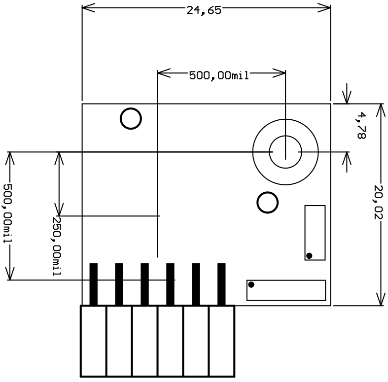
Figure 3: Board physical dimensions drawing.
Revision History
Hardware Revision History
| Date | Revision | Notes | PCN | Documentation Link |
|---|---|---|---|---|
| - | 01 | current available revision | - | TE0791-01 |
Table 5: Board hardware revision history.
Document Change History
| HTML |
|---|
<!--
Generate new entry:
1.add new row below first
2.Copy "Page Information Macro(date)" Macro-Preview, Metadata Version number, Author Name and description to the empty row. Important Revision number must be the same as the Wiki document revision number
3.Update Metadata = "Page Information Macro (current-version)" Preview+1 and add Author and change description.
--> |
Date | Revision | Contributors | Description | ||||||||
|---|---|---|---|---|---|---|---|---|---|---|---|
| Ali Naseri | initial document |
Table 6: Document change history.
Disclaimer
| Include Page | ||||
|---|---|---|---|---|
|
Some sources available on XMOD-JST-HEADER
Overview
Content Tools