Page History
...
| Scroll Only (inline) |
|---|
Refer to https://shopwiki.trenz-electronic.de/en/Download/?path=Trenz_Electronic/carrier_boards/TEBF0808/REV04 for downloadabledisplay/PD/TEBF0808+TRM for the current online version of this manual and additionalother technicalavailable documentation of the product. |
The Trenz Electronic TEBF0808 carrier board is a baseboard for the Xilinx Zynq Ultrascale+ MPSoC modules TE0808 and TE0803, which exposes the module's B2B connector pins to accessible connectors and provides a whole range of on-board components to test and evaluate the Zynq Ultrascale+ SoMs and for developing purposes. The carrier board has a Mini-ITX form factor making it capable to be fitted into a PC enclosure. On the PC enclosure's rear and front panel, MGT interfaces and connectors are accessible, for the front panel elements there are also Intel-PC compatible headers available.
...
The MGT-banks have also clock input-pins which are exposed to the FMC connector. Following MGT-lanes are available on the FMC connectors J5:
| B2B | Count Schematic Names of the MGT LanesSignals | Schematic Names / B2B Connector Pins | MGT Bank's Reference Clock Inputs from FMC Connector | J1 | 4 lanesPins | |||||||
|---|---|---|---|---|---|---|---|---|---|---|---|---|
B228_RX3_P, B228_RX3_N | , pins J5-A10, J5-A11
| , pins J5-A30, J5-A31B228_RX2_P, B228_RX2_N | , pins J5-A6, J5-A7
| , pins J5-A26, J5-A27B228_RX1_P, B228_RX1_N | , pins J5-A2, J5-A3
| , pins J5-A22, J5-A23B228_RX0_P, B228_RX0_N | , pins J5-C6, J5-C7
| , pins | J5J1- | C251, | J5-C31 MGT clock (B228_CLK0) from FMC connector | |
| J1 | 4 lanes | B229_RX3_P, B229_RX3_N, pins J5-B12, J5-B13 B229_RX2_P, B229_RX2_N, pins J5-B16, J5-B17 B229_RX1_P, B229_RX1_N, pins J5-A18, J5-A19 B229_RX0_P, B229_RX0_N, pins J5-A14, J5-A15 | 1 MGT clock (B229_CLK0) from FMC connector | |||||||||
| J1 | 2 lanes | B230_RX1_P, B230_RX1_N, pins J5-B4, J5-B5 B230_RX0_P, B230_RX0_N, pins J5-B8, J5-B9 | - |
...
The FMC connector provides pins for reference clock output to the Mezzanine module and clock input to PL banks of the MPSoC:
...
The FMC connector provides further interfaces like JTAG and I²C interfaces:
...
FMC_TCK, pin J5-D29
FMC_TMS, pin J5-D33
FMC_TDI, pin J5-D30
FMC_TDO, pin J5- D31
...
VCCIO: 3V3SB
TRST_L, pin J5-D34 pulled-up to 3V3_PER
...
FMC_SCL, pin J5-C30
FMC_SDA, pin J5-C31
...
I²C-lines pulled-up to 3V3_PER
...
FMC_PRSNT_M2C, pin J5-H2
FMC_PG_C2M, pin J5-D1 (3V3_PER pull-up)
FMC_PG_M2C, pin J5-F1 (3V3_PER pull-up)
FMC_CLK_DIR, pin J5-B1 (pulled-down to GND)
...
I²C I/O Expander U38
SC CPLD U39, bank 0
I²C I/O Expander U38
SC CPLD U17, bank 1
...
'PG' = 'Power Good'-signal
'C2M' = carrier to (Mezzanine) module
'M2C' = (Mezzanine) module to carrier
J1-53 pins J1-57, J1-59 pins J1-63, J1-65 pins J1-69, J1-71 | pins J5-A10, J5-A11 pins J5-A6, J5-A7 pins J5-A2, J5-A3 pins J5-C6, J5-C7 | |
B229_RX3_P, B229_RX3_N B229_RX2_P, B229_RX2_N B229_RX1_P, B229_RX1_N B229_RX0_P, B229_RX0_N | pins J1-27, J1-29 pins J1-33, J1-35 pins J1-39, J1-41 pins J1-45, J1-47 | pins J5-B12, J5-B13 pins J5-B16, J5-B17 pins J5-A18, J5-A19 pins J5-A14, J5-A15 |
B230_RX1_P, B230_RX1_N B230_RX0_P, B230_RX0_N | pins J1-15, J1-17 pins J1-21, J1-23 | pins J5-B4, J5-B5 pins J5-B8, J5-B9 |
Table 4: FMC connector pin-outs of available MGT lanes of the MPSoC
The FMC connector provides pins for reference clock output to the Mezzanine module and clock input to PL banks of the MPSoC:
| Clock Signal Schematic Name | FMC Connector Pins | Direction | Clock Source | Notes |
|---|---|---|---|---|
| B228_CLK0 | J5-D4 / J5-D5 | in | FMC Connector J5 | Extern MGT clock |
| B229_CLK0 | J5-B20 / J5-B21 | in | FMC Connector J5 | Extern MGT clock |
| FMCCLK2 | J5-K4 / J5-K5 | out | Carrier Board PLL SI5338A U35, CLK2 | Clock signal to Mezzanine module |
| FMCCLK3 | J5-J2 / J5-J3 | out | Carrier Board PLL SI5338A U35, CLK3 | Clock signal to Mezzanine module |
| B64_L14_P / B64_L14_N | J5-H4 / J5-H5 | in | FMC Connector J5 | Extern LVDS clock to PL bank |
| B48_L6_P / B48_L6_N | J5-G2 / J5-G3 | in | FMC Connector J5 | Extern LVDS clock to PL bank |
Table 5: FMC connector pin-outs for reference clock output
The FMC connector provides further interfaces like JTAG and I²C interfaces:
| Interfaces | I/O Signal Count | Pin schematic Names / FMC Pins | Connected to | Notes |
|---|---|---|---|---|
| JTAG | 5 | FMC_TCK, pin J5-D29 FMC_TMS, pin J5-D33 FMC_TDI, pin J5-D30 FMC_TDO, pin J5- D31 | SC CPLD U17, bank 1 | VCCIO: 3V3SB TRST_L, pin J5-D34 pulled-up to 3V3_PER |
| I²C | 2 | FMC_SCL, pin J5-C30 FMC_SDA, pin J5-C31 | I²C Switch U16 | I²C-lines pulled-up to 3V3_PER |
| Control Lines | 4 | FMC_PRSNT_M2C, pin J5-H2 | I²C I/O Expander U38 | 'PG' = 'Power Good'-signal 'C2M' = carrier to (Mezzanine) module 'M2C' = (Mezzanine) module to carrier |
| FMC_PG_C2M, pin J5-D1 (3V3_PER pull-up) | SC CPLD U39, bank 0 | |||
| FMC_PG_M2C, pin J5-F1 (3V3_PER pull-up) | I²C I/O Expander U38 | |||
| FMC_CLK_DIR, pin J5-B1 (pulled-down to GND) | SC CPLD U17, bank 1 |
Table 6: FMC connector pin-outs of available interfaces to the System Controller CPLD
Several VCCIO voltages are available on the FMC connector to operate the I/O's on different voltage levels:
| VCCIO Schematic Name | FMC Connector J5 Pins | Notes |
|---|---|---|
| 12V | C35/C37 | extern 12V power supply |
| 3V3_PER | D32/D36/D38/D40/C39 | 3.3V peripheral supply voltage |
| FMC_VADJ | H40/G39/F40/E39 | adjustable FMC VCCIO voltage, supplied by DC-DC converter U8 |
Table 7: Available VCCIO voltages on FMC connector
MIO Bank Interfaces
The TEBF0808 carrier board provides several interfaces, which are configured on the MIO banks 500 .. 503 of the Zynq Ultrascale+ MPSoC.
Following table contains the assignment of the MIO pins to the configured interfaces:
| MIO | Configured as | System Controller CPLD | Notes |
|---|---|---|---|
| 0..12 | Dual QSPI | - | Dual Flash Memory on TE0808 / TE0803 SoM; Bootable |
| 13..23 | SD0: eMMC | - | eMMC Memory U2; Bootable |
| 24, 25 | - | CPLD (U39) MUXED | - |
| 26..29 | - | CPLD (U17 MUXED | Bootable JTAG (PJTAG0) |
| 30 | force reboot after FSBL-PLL config for PCIe | CPLD (U39) MUXED | - |
| 31 | PCIe reset | CPLD (U39) MUXED | - |
| 32 | - | CPLD (U39) MUXED | - |
| 33 | - | CPLD (U39) MUXED | - |
| 34..37 | - | CPLD (U39) MUXED | - |
| 38, 39 | I2C0 | - | - |
| 40 | forwarded to PWRLED_P / LED_P | CPLD (U39) MUXED | - |
| 41 | - | - | - |
| 42, 43 | UART0 | CPLD (U39) MUXED | - |
| 44 | SD_WP to FPGA | CPLD (U39) MUXED | - |
| 45..51 | SD1: SD | - | Bootable MikroSD / MMC Card |
| 52..63 | USB0 | - | - |
| 64..75 | GEM3 | - | Ethernet RGMII |
| 76, 77 | MDC / MDIO | - | Ethernet RGMII |
Table 8: MIO Assignment
Following interfaces are provided by the MIO bank of the Zynq Ultrascale+ MPSoC:
- 4x USB3.0 Superspeed ports (downward compatible to USB2.0 Highspeed)
- SDIO port with muxed MikroSD and MMC Card socket
- Gigabit Ethernet interface connected per RGMII
- eMMC interface
- Master I²C interface to on-board peripherals
The block-diagram below visualizes the interfaces of the MIO bank at the Zynq Ultrascale+ MPSoC and their associated on-board peripherals.
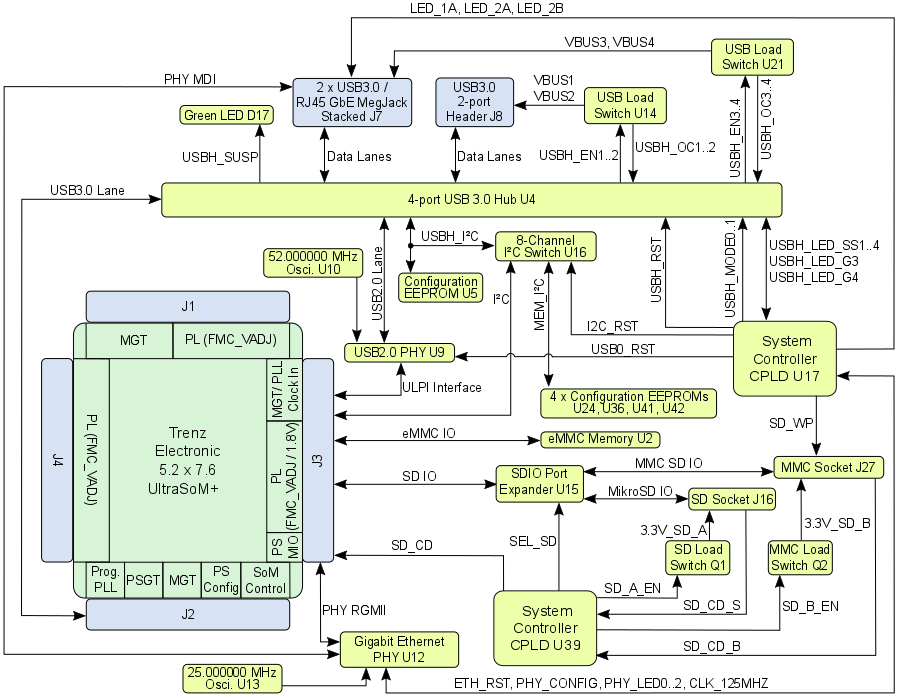
Figure 4: TEBF0808 MIO Interfaces
PS GT Bank Interfaces
The PS GT Bank 505 provides beside the USB3.0 Lane also following interfaces:
- SATA (PS GT bank, MGT2 Lane)
- DisplayPort (PS GT bank, MGT3 Lane, only TX-pair routed)
- PCI Express (PS GT bank, MGT0 Lane)
| Function | MGT Lane | Schematic Names / B2B pins | Required Ref Clock | Clock Source | Comment |
|---|---|---|---|---|---|
| PCIe | PS 0 | PCI_TX_N, pin J2-67 PCI_RX_N, pin J2-70 | 100 MHz | clock signal of SoM's prog. PLL | single lane PCIe connector clock signal routed on carrier board to PCIe connector J1 |
| USB3 | PS 1 | USB3_TXUP_N, pin J2-61 USB3_RXUP_N, pin J2-64 | 100 MHz | clock signal of SoM's prog. PLL | clock signal routed on-module, |
| SATA | PS 2 | SATA_TX_N, pin J2-55 SATA_RX_N, pin J2-58 | 150 MHz | On-board oscillator U23 | optional: clock signal of SoM's prog. PLL |
| DP.0 | PS 3 | DP0_TX_N, pin J2-49 | 27 MHz | clock signal of SoM's prog. PLL | DisplayPort GT SERDES clock signal, |
Table 9: PS GT Lane Assignment
Following block diagram shows the wiring of the MGT Lanes of the PS GT bank 505 to the particular high speed data interfaces:
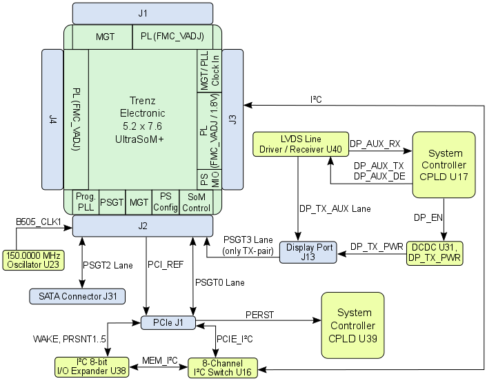
Figure 5: TEBF0808 PS GT Bank 505 Interface
Follwowing table contains a brief description of the control and status signals of PCIe interface:
| Signal Schematic Name | FPGA Direction | Description | Logic |
|---|---|---|---|
| WAKE | Input | Link reactivation | Low active |
| PERST | Input | PCI Express reset input | Low active |
| PRSNT1 | Input | Reference pin for PCIe card lane size | - |
| PRSNT2 | Input | PCI Express ×1 cards | connect to PRSNT1 |
| PRSNT3 | Input | PCI Express ×4 cards | connect to PRSNT1 |
| PRSNT4 | Input | PCI Express ×8 cards | connect to PRSNT1 |
| PRSNT5 | Input | PCI Express ×16 cards | connect to PRSNT1 |
| PCIE_I²C | BiDir | 2-wire PCIE System Management Bus | - |
Table 10: Description of MGT Connectors Control and Status Signals
MGT Interfaces SFP+ and FireFly
The TEBF0808 carrier board provides the high speed MGT interface connectors "SFP+" (Enhanced small form-factor pluggable) and Samtec "FireFly". This connectors are capable of data transmission rates up to 10 Gbit/s with SFP+ and 28 Gbit/s with FireFly.
| Function | MGT Lane | Schematic Names / B2B pins | Required Ref Clock | Clock Source | Comment |
|---|---|---|---|---|---|
| FireFly | MGT Lanes 0..3 | B128_RX3_N, B128_RX3_P, pins J2-28, J2-30 B128_RX2_N, B128_RX2_P, pins J2-34, J2-36 B128_RX1_N, B128_RX1_P, pins J2-40, J2-42 B128_RX0_N, B128_RX0_P, pins J2-46, J2-48 |
...
Several VCCIO voltages are available on the FMC connector to operate the I/O's on different voltage levels:
...
Table 7: Available VCCIO voltages on FMC connector
MIO Bank Interfaces
The TEBF0808 carrier board provides several interfaces, which are configured on the MIO banks 500 .. 503 of the Zynq Ultrascale+ MPSoC.
Following table contains the assignment of the MIO pins to the configured interfaces:
...
Following interfaces are provided by the MIO bank of the Zynq Ultrascale+ MPSoC:
- 4x USB3.0 Superspeed ports (downward compatible to USB2.0 Highspeed)
- SDIO port with muxed MikroSD and MMC Card socket
- Gigabit Ethernet interface connected per RGMII
- eMMC interface
- Master I²C interface to on-board peripherals
The block-diagram below visualizes the interfaces of the MIO bank at the Zynq Ultrascale+ MPSoC and their associated on-board peripherals.
Figure 4: TEBF0808 MIO Interfaces
PS GT Bank Interfaces
The PS GT Bank 505 provides beside the USB3.0 Lane also following interfaces:
...
single lane PCIe connector
clock signal routed on carrier board to PCIe connector J1
...
clock signal routed on-module,
also optional (not equipped) 100 MHz osci. U35 configurable
...
optional: clock signal of SoM's prog. PLL
...
DisplayPort GT SERDES clock signal,
routed on-module to MGT bank
Table 9: PS GT Lane Assignment
Following block diagram shows the wiring of the MGT Lanes of the PS GT bank 505 to the particular high speed data interfaces:
...
Follwowing table contains a brief description of the control and status signals of PCIe interface:
...
Table 10: Description of MGT Connectors Control and Status Signals
MGT Interfaces SFP+ and FireFly
The TEBF0808 carrier board provides the high speed MGT interface connectors "SFP+" (Enhanced small form-factor pluggable) and Samtec "FireFly". This connectors are capable of data transmission rates up to 10 Gbit/s with SFP+ and 28 Gbit/s with FireFly.
| Function | MGT Lane | Required Ref Clock | Clock Source | Comment | |
|---|---|---|---|---|---|
| FireFly | MGT Lanes 0..3 | - | clock signal of SoM's prog. PLL | clock signal on-module routed to MGT bank | |
| SFP | MGT Lane 2 | B230_RX2_P, pin J1-9 B230_TX2_P, pin J1-8 | 125 / 156.25 MHz | clock signal of SoM's prog. PLL | clock signal routed on carrier board to MGT bank |
| SFP | MGT Lane 3 | B230_RX3_P, pin J1-3 B230_TX3_P, pin J1-2 | 125 / 156.25 MHz | clock signal of SoM's prog. PLL | clock signal routed on carrier board to MGT bank |
...
Overview
Content Tools