Page History
...
Main Components
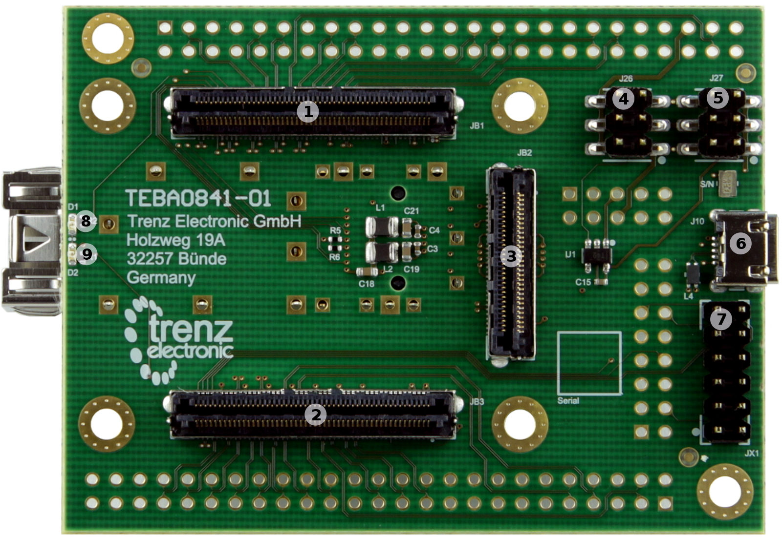
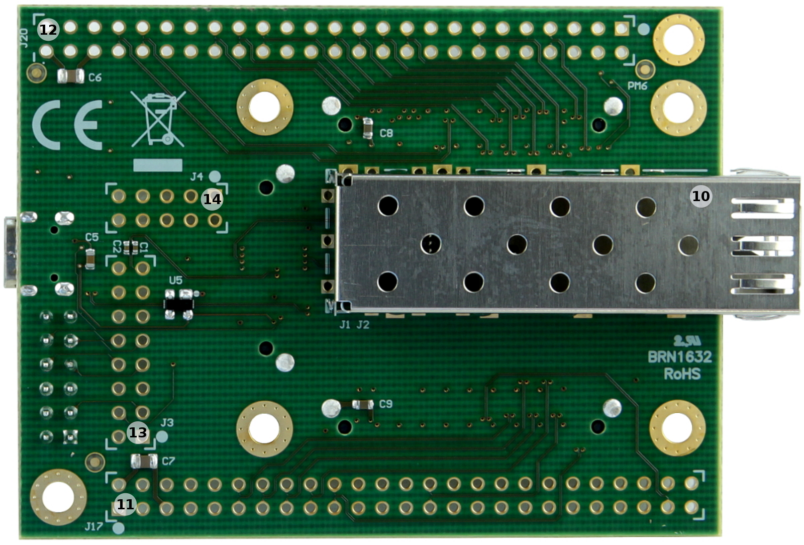
Figure 2: TE0706TEBA0841-02 01 Carrier Board.
- Samtec Razor Beam™ LSHM-150 B2B connector, JB1
- Samtec Razor Beam™ LSHM-150 B2B connector, JB3
- Samtec Razor Beam™ LSHM-130 B2B connector, JB2
- 6-pin header J26, for selecting PL I/O-bank voltage
- 6-pin header J27, for selecting PL I/O-bank voltage
- Micro USB2.0 Type B Connector J12 (Device or OTG mode)
- JTAG/UART header, JX1 ('XMOD FTDI JTAG Adapter'-compatible pin-assignment)
- User LED D1 (green)
- User LED D2 (red)
- SFP+ Connector, J1
- 50-pin header soldering-pads J17, for access to PL I/O-bank pins (LVDS-pairs possible)
- 50-pin header soldering-pads J20, for access to PL I/O-bank pins (LVDS-pairs possible)
- 16-pin header soldering-pads J3, JTAG/UART header ('XMOD FTDI JTAG Adapter'-compatible pin-assignment)
- 10-pin header soldering-pads J4, for access to SoM's SDIO-port, if available
...
| SFP+ pin | Pin Schematic Name | B2B | FPGA Direction | Description | Note |
|---|---|---|---|---|---|
| Transmit Data + (pin 18) | MGT_TX3_P | JB2-26 | Output | SFP+ transmit data differential pair | - |
| Transmit Data - (pin 19) | MGT_TX3_N | JB2-28 | Output | - | |
| Receive Data + (pin 13) | MGT_RX3_P | JB2-25 | Input | SFP+ receive data differential pair | - |
| Receive Data - (pin 12) | MGT_RX3_N | JB2-27 | Input | - | |
| Receive Fault (pin 2) | MIO10 | JB1-96 | Input | Fault / Normal Operation | High active logic |
| Receive disable (pin 3) 1) | SFP0_TX_DIS | not connected | Output | SFP Enabled / Disabled | Low active logic |
| MOD-DEF2 (pin 4) | MIO13 | JB1-98 | Input | Module present / not present | Low active logic |
| MOD-DEF1 (pin 5) | MIO12 | JB1-100 | Output | 2-wire Serial Interface clock | 3.3V pull-up on-board |
| MOD-DEF0 (pin 6) | MIO11 | JB1-94 | BiDir | 2-wire Serial Interface data | 3.3V pull-up on-board |
| RS0 (pin 7) | SFP0_RS0 | not connected | Output | Full RX bandwidth | Low active logic |
| LOS (pin 8) | MIO0 | JB1-88 | Input | Loss of receiver signal | High active logic |
| RS1 (pin 9) | SFP0_RS1 | not connected | Output | Reduced RX bandwidth | Low active logic |
Table 13: SFP+ connector pin-assignment.
...
| MGT Lane | B2B TX Differential Pair | B2B RX Differential Pair | B2B Pins Bridged |
|---|---|---|---|
| MGT-lane 0 | JB2-8 (MGT_TX0_N) JB2-10 (MGT_TX0_P) | JB2-7 (MGT_RX0_N) JB2-9 (MGT_RX0_P) | JB2-7 to JB2-8 JB2-9 to JB2-10 |
| MGT-lane 1 | JB2-14 (MGT_TX1_N) JB2-16 (MGT_TX1_P) | JB2-13 (MGT_RX1_N) JB2-15 (MGT_RX1_P) | JB2-13 to JB2-14 JB2-15 to JB2-16 |
| MGT-lane 2 | JB2-20 (MGT_TX2_N) JB2-22 (MGT_TX2_P) | JB2-19 (MGT_RX2_N) JB2-21 (MGT_RX2_P) | JB2-19 to JB2-20 JB2-21 to JB2-22 |
| MGT-lane 7 | JB1-3 (MGT_TX7_P) JB1-5 (MGT_TX7_N) | JB1-9 (MGT_RX7_P) JB1-11 (MGT_RX7_N) | JB1-3 to JB1-9 JB1-5 to JB1-11 |
| MGT-lane 6 | JB1-15 (MGT_TX6_P) JB1-17 (MGT_TX6_N) | JB1-21 (MGT_RX6_P) JB1-23 (MGT_RX6_N) | JB1-15 to JB1-21 JB1-17 to JB1-23 |
Table 24: Looped-backed MGT-lanes for mounted 4 x 5 SoM TE0741.
...
JTAG Signal | B2B Connector Pin | XMOD Header JX1 | Pin Header J3 | Note |
|---|---|---|---|---|
| TCK | JB3-100 | JX1-4 | J3-4 | - |
| TDI | JB3-96 | JX1-10 | J3-10 | - |
| TDO | JB3-98 | JX1-8 | J3-8 | - |
| TMS | JB3-94 | JX1-12 | J3-12 | - |
Table 35: JTAG interface signals.
UART Interface
...
| UART Signal Schematic Name | B2B | XMOD Header JX1 | Pin Header J3 | Note |
|---|---|---|---|---|
| MIO14 | JB1-91 | JX1-7 | J3-7 | UART-RX (receive line) |
| MIO15 | JB1-86 | JX1-3 | J3-3 | UART-TX (transmit line) |
Table 46: UART interface signals.
SD IO Interface
...
| SD IO Signal Schematic Name | B2B | Pin Header J4 | Note |
|---|---|---|---|
| SD_DAT0 | JB1-24 | J4-8 | SD IO data |
| SD_DAT1 | JB1-22 | J4-10 | SD IO data |
| SD_DAT2 | JB1-20 | J4-9 | SD IO data |
| SD_DAT3 | JB1-18 | J4-7 | SD IO data |
| SD_CLK | JB1-28 | J4-4 | SD IO clock |
| SD_CMD | JB1-26 | J4-3 | SD IO command |
Table 67: SD IO interface signals.
...
| USB2.0 Signal Schematic Name | B2B | Connected to | Note |
|---|---|---|---|
| OTG_N | JB2-48 | J10-2 | USB2.0 data |
| OTG_P | JB2-50 | J10-3 | USB2.0 data |
| OTG-ID | JB2-52 | J10-4 | Ground this pin for A-Device (host), left floating this pin for B-Device (peripheral). |
| USB-VBUS | JB2-56 | J10-1 | USB supply voltage for Host mode. Not supplied by the Carrier Board. |
Table 78: USB2.0 interface signals and connections.
...
| Pin Schematic Name | XMOD Header JX1 Pin | Header J3 Pin | B2B | Note |
|---|---|---|---|---|
| TCK | C (pin 4) | 4 | JB3-100 | - |
| TDO | D (pin 8) | 8 | JB3-98 | - |
| TDI | F (pin 10) | 10 | JB3-96 | - |
| TMS | H (pin 12) | 12 | JB3-94 | - |
| MIO15 | A (pin 3) | 3 | JB1-86 | UART-TX (transmit line) |
| MIO14 | B (pin 7) | 7 | JB1-91 | UART-RX (receive line) |
| BOOTMODE | E (pin 9) | 9 | JB1-90 | usually 'JTAGSEL' on TE 4 x 5 SoMs |
| RESIN | G (pin 11) | 11 | JB3-17 | SoM Reset pin |
| CLK0_N | - | 15 | JB2-32 | AC decoupled on-board (100 nF capacitor) |
| CLK0_P | - | 16 | JB2-34 | AC decoupled on-board (100 nF capacitor) |
Table 109: JTAG/UART header signals and connections.
...
| XMOD DIP-switches | Position |
|---|---|
| Switch 1 | ON |
| Switch 2 | OFF |
| Switch 3 | OFF |
| Switch 4 | OFF |
Table 1110: XMOD adapter board DIP-switch positions for voltage configuration.
...
The on-board LEDs are available to the user and can be used to indicate system status and activities:
| LED | Color | Pin Schematic Name | B2B Connector | Description and Notes |
|---|---|---|---|---|
| D1 | Green | MIO9 | JB1-92 | available to user |
| D2 | Red | RLED | JB3-90 | available to user |
Figure 311: On-board LEDs
VCCIO Selection Jumper
...
TE 4 x 5 Modules have a standard assignment of PL-bank I/O voltages on their B2B connectors, which will be fed with I/O voltage from base-board.
Base-board PL-bank I/O Voltages | B2B Pins | Standard Assignment of PL-bank I/O Voltages on TE 4x5 Modules |
|---|---|---|
| VCCIOA | JB1-10, JB1-12 | VCCIOA (JM1-9, JM1-11) |
| VCCIOD | JB2-8, JB2-10 | VCCIOD (JM2-7, JM2-9) |
Table 512: Base-board PL-bank I/O voltages VCCIOA and VCCIOD
...
Following table describes how to configure the base-board supply-voltages by jumpers:
Base-board PL-bank I/O Voltages | VCCIOA | VCCIOD |
|---|---|---|
| 1.8V | J26:1-2 | J27:1-2 |
| 2.5V | J26:3-4 | J27:3-4 |
| 3.3V | J26:5-6 | J27:5-6 |
Table 613: Configuration of base-board supply-voltages via jumpers. Jumper-Notification: 'Jx: 1-2' means pins 1 and 2 are connected, 'Jx: 3-4' means pins 3 and 4 are connected, and so on.
...
The external power-supply can be connected to the board by the following pins:
| Connector | 3.3V pin | GND pin |
|---|---|---|
| JX1 | JX1-5, JX1-6, | JX1-1, JX1-2 |
| J3 | J3-5, J3-6 | J3-1, J3-2 |
| J4 | J4-5 | J4-1, J4-2 |
| J20 | J20-5, J20-46 | J20-1 , J20-2 , J20-49 , J20-50 |
| J17 | J17-5, J17-46 | J17-1 , J17-2 , J17-49 , J17-50 |
Table 415: Connector pins capable for external 3.3V power supply
...
Following diagram shows the distribution of the external input voltage of nominal 3.3V to the components:
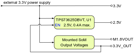
Figure 54: Board power distribution diagram.
...
| Module Connector (B2B) Designator | VCC / VCCIO | Direction | Pins | Notes |
|---|---|---|---|---|
| JB1 | 3.3V | Out | 2, 4, 6, 14, 16 | 3.3V module supply voltage |
| VCCIOA | Out | 10, 12 | PL IO-bank VCCIO | |
| M1.8VOUT | In | 40 | 1.8V module output voltage | |
| JB2 | 3.3V_OUT | In | 9, 11 | 3.3V module output voltage |
| 3.3V | Out | 1, 3, 5, 7 | 3.3V module supply voltage | |
| VCCIOD | Out | 8, 10 | PL IO-bank VCCIO | |
| JB3 | USB-VBUS | Out | 56 | USB Host supply voltage |
Table 1516: Power pin description of B2B module connector.
...
| On-board Pin Header Designator | VCC / VCCIO | Direction | Pins | Notes |
|---|---|---|---|---|
| J17 | 3.3V | In / Out | 5, 48 | 3.3V external supply voltage |
| VCCIOD | In / Out | 6, 45 | PL IO-bank VCCIO, depends on Jumper settings | |
| J20 | 3.3V | In / Out | 5, 48 | 3.3V external supply voltage |
| VCCIOA | In / Out | 6, 45 | PL IO-bank VCCIO, depends on Jumper settings |
Table 1617: Power Pin description of on-board connector.
...
| Jumper / Header Designator | VCC / VCCIO | Direction | Pins | Notes |
|---|---|---|---|---|
| J26 | VCCIOA | In | 2, 4, 6 | - |
| M1.8VOUT | Out | 1 | - | |
| 2.5V | Out | 3 | - | |
| 3.3V_OUT | Out | 5 | - | |
| J27 | VCCIOD | In | 2, 4, 6 | - |
| M1.8VOUT | Out | 1 | - | |
| 2.5V | Out | 3 | - | |
| 3.3V_OUT | Out | 5 | - | |
| J4 | 3.3V | Out | 5 | - |
| M1.8VOUT | Out | 6 | - |
Table 1718: Power Pin description of VCCIO selection jumper pin header.
...
Technical Specifications
Absolute Maximum Ratings
| Parameter | Min | Max | Units | Notes |
|---|---|---|---|---|
Vin supply voltage | 3.135 | 3.465 | V | 3.3V supply-voltage ± 5% |
Storage Temperature | -55 | 105 | °C | Molex 74441-0001 Product Specification |
Table 2221: Board absolute maximum ratings.
Recommended Operating Conditions
| Parameter | Min | Max | Units | Notes |
|---|---|---|---|---|
| Vin supply voltage | 3.135 | 3.465 | V | - |
| Operating temperature | -40 | +85 | °C | Molex 74441-0001 Product Specification |
Table 2322: Module recommended operating conditions.
...
The dimensions are given in mm and mil (milli inch).
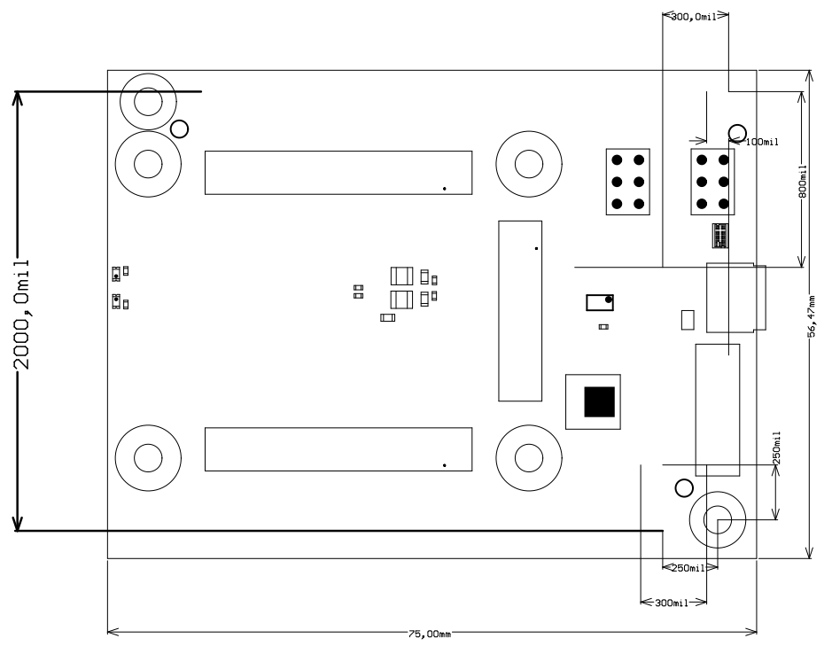
Figure 65: Board physical dimensions drawing.
...
| Date | Revision | Notes | PCN | Documentation Link |
|---|---|---|---|---|
| - | 01 |
| - | TEBA0841-01 |
Table 2423: Module hardware revision history.
Hardware revision number can be found on the PCB board together with the module model number separated by the dash.
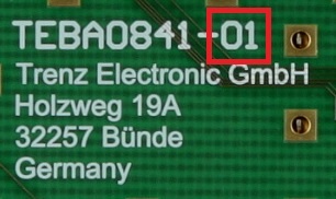
Figure 76: Board hardware revision number.
...
Date | Revision | Contributors | Description | ||||||||
|---|---|---|---|---|---|---|---|---|---|---|---|
| Ali Naseri, Jan Kumann |
|
Table 2524: Document change history.
...
Overview
Content Tools