Download PDF version of this document.
Table of Contents
Overview
The Trenz Electronic TEBA0841 is a Carrier Board for testing, evaluation and development purposes, especially for the Multi-gigabit transceiver units of the TE0841 and TE0741 modules. Although this base-board is dedicated to the modules TE0841 and TE0741, it is also compatible with other Trenz Electronic 4 x 5 cm SoMs.
See page "4 x 5 cm carriers" to get information about the SoMs supported by the TEBA0841 base-board.
Key Features
- SFP+ connector (Enhanced small form-factor pluggable), supports data transmission rates up to 10 Gbit/s
- Micro USB2.0 Type B Connector (J10)
- Trenz 4x5 module Socket (3 x Samtec LSHM series connectors)
- 4 x 5 SoM programmable by XMOD JTAG/UART header (JX1)
- 2 x user LEDs routed to I/O-pins of the SoM
- Soldering-pads J17 and J20 for optional pin headers for access to SoM's I/O-bank-pins, usable as LVDS-pairs
- Soldering-pads J3 and J4 for optional pin headers for access to further interfaces and I/O's of the SoM
Additional assembly options are available for cost or performance optimization upon request.
Block Diagram
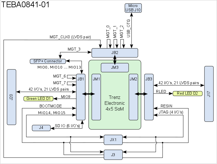
Figure 1: TEBA0841-01 Block Diagram.
Main Components
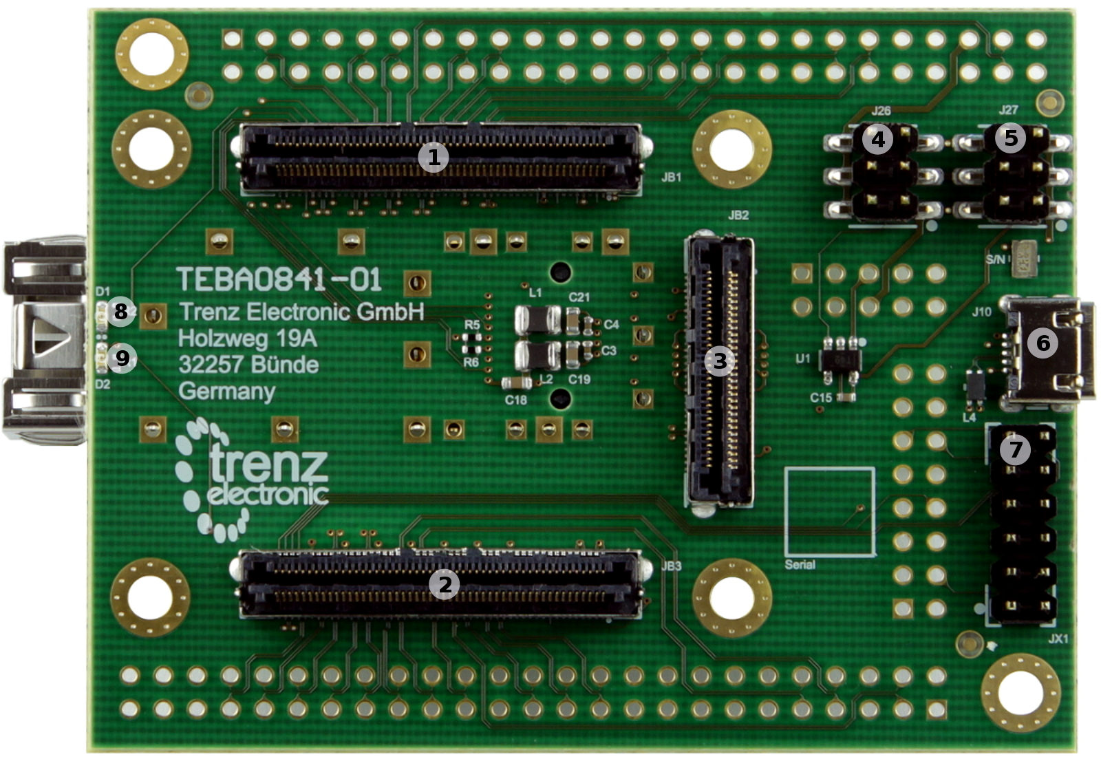
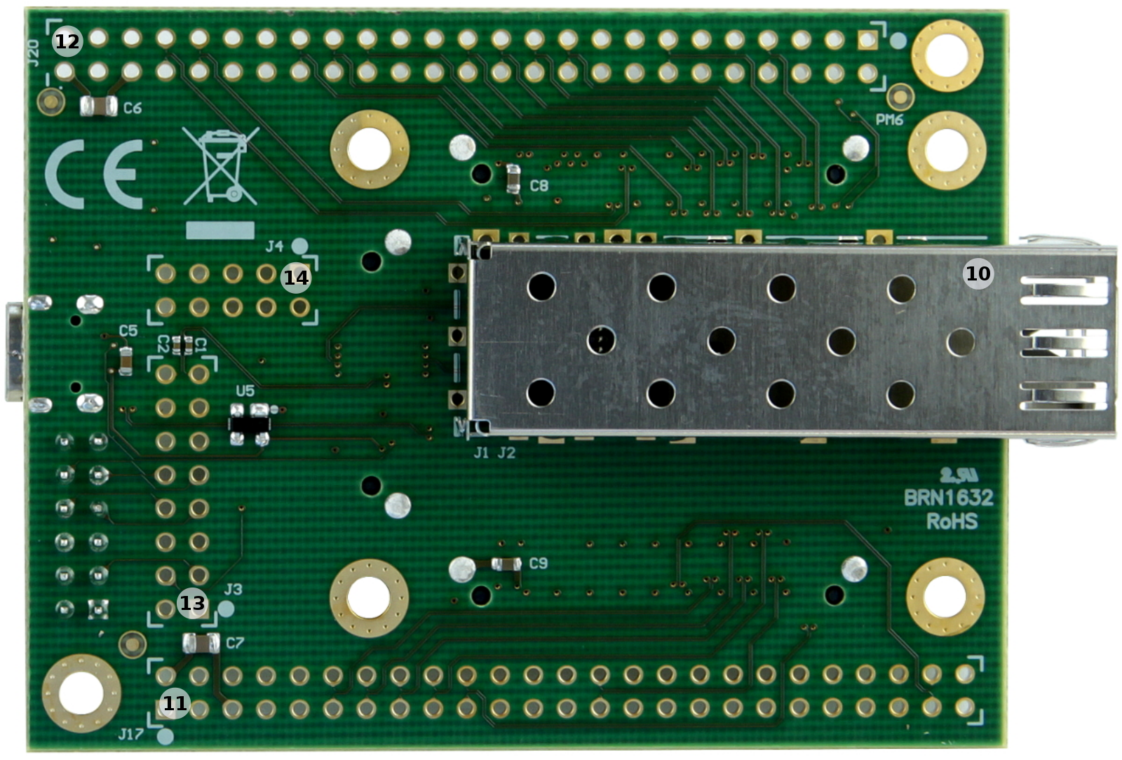
Figure 2: TE0706-02 Carrier Board.
- Samtec Razor Beam™ LSHM-150 B2B connector, JB1
- Samtec Razor Beam™ LSHM-150 B2B connector, JB3
- Samtec Razor Beam™ LSHM-130 B2B connector, JB2
- 6-pin header J26, for selecting PL I/O-bank voltage
- 6-pin header J27, for selecting PL I/O-bank voltage
- Micro USB2.0 Type B Connector J12 (Device or OTG mode)
- JTAG/UART header, JX1 ('XMOD FTDI JTAG Adapter'-compatible pin-assignment)
- User LED D1 (green)
- User LED D2 (red)
- SFP+ Connector, J1
- 50-pin header soldering-pads J17, for access to PL I/O-bank pins (LVDS-pairs possible)
- 50-pin header soldering-pads J20, for access to PL I/O-bank pins (LVDS-pairs possible)
- 16-pin header soldering-pads J3, JTAG/UART header ('XMOD FTDI JTAG Adapter'-compatible pin-assignment)
- 10-pin header soldering-pads J4, for access to SoM's SDIO-port, if available
Initial Delivery State
Board is shipped in following configuration:
- VCCIO voltage selection jumpers are all set to 1.8 V.
- Pin headers (not soldered to the board, but included in the package as separate component)
Different delivery configurations are available upon request.
Signals, Interfaces and Pins
B2B Connector
With the TEBA0841 Carrier Board's Board-to-Board Connectors (B2B) the MIO- and PL I/O-bank's pins and further interfaces of the mounted SoM can be accessed. A large quantity of these I/O's are also usable as differential pairs. The connectors provide also VCCIO voltages to operate the I/O's properly.
Following table gives a summary of the available I/O's, interfaces and differential pairs of the B2B connectors JB1, JB2 and JB3:
| B2B Connector | Interfaces | Count of I/O's | Notes |
|---|---|---|---|
| JB1 | User I/O | 42 single ended or 21 differential | - |
| SD IO | 6 | - | |
| MIO | 8 | - | |
| SoM control signals | 1 | 'BOOTMODE' | |
| JB2 | MGT lanes | 8 differential pairs, 4 lanes | - |
| MGT reference input clock | 1 differential pair | ||
| USB2.0 (OTG and device mode) | 4 | - | |
| JB2 | User I/O | 42 single ended 21 differential | -- |
| JTAG | 4 | - | |
| Red user LED | 1 | - | |
| SoM control signals | 1 | 'RESIN' |
Table 1: General overview of PL I/O signals and SoM's interfaces connected to the B2B connectors.
On-board Pin Header
The TEBA0841 Carrier Board has 4 footprints as soldering pads to mount 2.54mm grid size pin headers to get access the PL I/O-bank's pins and further interfaces of the mounted SoM. With these pin headers, SoM's PL-I/O's are available to the user, a large quantity of these I/O's are also usable as differential pairs.
Following table gives a summary of the pin-assignment, available interfaces and functional I/O's of the pin headers:
| On-board Pin Header | Control Signals and Interfaces | Count of I/O's | Notes |
|---|---|---|---|
| J17 | User I/O | 42 single ended or 21 differential | - |
| J20 | User I/O | 42 single ended or 21 differential | - |
| J3 | JTAG | 4 | - |
| SoM control signals | 2 | 'RESIN', 'BOOTMODE' | |
| MGT reference input clock | 1 differential pair | AC decoupled on-board (100 nF capacitor) | |
| MIO | 2 | user IO (configurable as UART for example) | |
| J4 | SD IO | 6 | 3.3V and 1.8V voltage level available on header |
Table 2: General overview of PL I/O signals, SoM's interfaces and control signals connected to the on-board connectors.
SFP+ Connector
On the TEBA0841 carrier board is a SFP+ connector J1 (board-rev. 01: Molex 74441-0001). The connector is embedded into a SFP cage J2 (board-rev. 01: Molex 74737-0009).
The differential RX/TX data lanes are connected to B2B connector JB2, the control-lines are connected to B2B connector JB1 and are assigned to MIO-bank pins of the mounted SoM.
The pin-assignment of the SFP connector is in detail as fellows:
| SFP+ pin | Pin Schematic Name | B2B | FPGA Direction | Description | Note |
|---|---|---|---|---|---|
| Transmit Data + (pin 18) | MGT_TX3_P | JB2-26 | Output | SFP+ transmit data differential pair | - |
| Transmit Data - (pin 19) | MGT_TX3_N | JB2-28 | Output | - | |
| Receive Data + (pin 13) | MGT_RX3_P | JB2-25 | Input | SFP+ receive data differential pair | - |
| Receive Data - (pin 12) | MGT_RX3_N | JB2-27 | Input | - | |
| Receive Fault (pin 2) | MIO10 | JB1-96 | Input | Fault / Normal Operation | High active logic |
| Receive disable (pin 3) 1) | SFP0_TX_DIS | not connected | Output | SFP Enabled / Disabled | Low active logic |
| MOD-DEF2 (pin 4) | MIO13 | JB1-98 | Input | Module present / not present | Low active logic |
| MOD-DEF1 (pin 5) | MIO12 | JB1-100 | Output | 2-wire Serial Interface clock | 3.3V pull-up on-board |
| MOD-DEF0 (pin 6) | MIO11 | JB1-94 | BiDir | 2-wire Serial Interface data | 3.3V pull-up on-board |
| RS0 (pin 7) | SFP0_RS0 | not connected | Output | Full RX bandwidth | Low active logic |
| LOS (pin 8) | MIO0 | JB1-88 | Input | Loss of receiver signal | High active logic |
| RS1 (pin 9) | SFP0_RS1 | not connected | Output | Reduced RX bandwidth | Low active logic |
Table 1: SFP+ connector pin-assignment.
1) Important: For proper operation, a wire patch to GND is done at recently delivered boards. Connect to GND, if not done. See PCB drawing below:
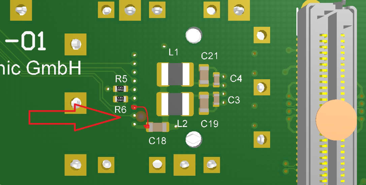
Figure 3: PCB wire patch for SFP+ connector.
Looped-backed MGT-Lanes on B2B Connector JB1 and JB2
The TEBA0841 carrier board is mainly designed for the 4 x 5 SoMs TE0841 and TE0741. This SoMs have GTX-Transceiver units on their FPGA-modules with up to 8 available MGT-lanes. To test this MGT-lanes, 5 RX/TX differential pairs are bridged on-board, hence the transmitted data on this MGT-lanes flows back to their sources in a loop-back circuit without intentional processing or modification.
The MGT lane pins are bridged on-board as fellows, if 4 x 5 SoM TE0741 is mounted on carrier board:
| MGT Lane | B2B TX Differential Pair | B2B RX Differential Pair | B2B Pins Bridged |
|---|---|---|---|
| MGT-lane 0 | JB2-8 (MGT_TX0_N) JB2-10 (MGT_TX0_P) | JB2-7 (MGT_RX0_N) JB2-9 (MGT_RX0_P) | JB2-7 to JB2-8 JB2-9 to JB2-10 |
| MGT-lane 1 | JB2-14 (MGT_TX1_N) JB2-16 (MGT_TX1_P) | JB2-13 (MGT_RX1_N) JB2-15 (MGT_RX1_P) | JB2-13 to JB2-14 JB2-15 to JB2-16 |
| MGT-lane 2 | JB2-20 (MGT_TX2_N) JB2-22 (MGT_TX2_P) | JB2-19 (MGT_RX2_N) JB2-21 (MGT_RX2_P) | JB2-19 to JB2-20 JB2-21 to JB2-22 |
| MGT-lane 7 | JB1-3 (MGT_TX7_P) JB1-5 (MGT_TX7_N) | JB1-9 (MGT_RX7_P) JB1-11 (MGT_RX7_N) | JB1-3 to JB1-9 JB1-5 to JB1-11 |
| MGT-lane 6 | JB1-15 (MGT_TX6_P) JB1-17 (MGT_TX6_N) | JB1-21 (MGT_RX6_P) JB1-23 (MGT_RX6_N) | JB1-15 to JB1-21 JB1-17 to JB1-23 |
Table 2: Looped-backed MGT-lanes for mounted 4 x 5 SoM TE0741.
Note: The mounted TE 4 x 5 SoMs have different schematic net-names of the differential signaling pairs of the MGT-lanes. See Schematic of the particular SoM.
JTAG Interface
JTAG access to the mounted SoM is provided through B2B connector JB2 and is also routed to the XMOD header JX1 and pin header J3. With the TE0790 XMOD USB2.0 to JTAG adapter, the device of the mounted SoM can be programed via USB2.0 interface.
JTAG Signal | B2B Connector Pin | XMOD Header JX1 | Pin Header J3 | Note |
|---|---|---|---|---|
| TCK | JB3-100 | JX1-4 | J3-4 | - |
| TDI | JB3-96 | JX1-10 | J3-10 | - |
| TDO | JB3-98 | JX1-8 | J3-8 | - |
| TMS | JB3-94 | JX1-12 | J3-12 | - |
Table 3: JTAG interface signals.
UART Interface
UART interface is available on B2B connector JB1 and is usually established by MIO-pins of the PS-bank of the mounted SoM's Zynq device. With the TE0790 XMOD USB2.0 adapter, the UART signals can be converted to USB2.0 interface signals:
| UART Signal Schematic Name | B2B | XMOD Header JX1 | Pin Header J3 | Note |
|---|---|---|---|---|
| MIO14 | JB1-91 | JX1-7 | J3-7 | UART-RX (receive line) |
| MIO15 | JB1-86 | JX1-3 | J3-3 | UART-TX (transmit line) |
Table 4: UART interface signals.
SD IO Interface
The SD IO interface of the mounted SoM is routed to the pin header J4. Due to the different operation voltage levels of the MicroSD Card socket (3.3V) and the and the SoM's Zynq device MIO-bank (1.8V), a VDD/VCCIO translation is necessary which can be provided for example by Texas Instruments TXS02612 SDIO port expander IC. Both voltage levels are available on pin header J4:
| SD IO Signal Schematic Name | B2B | Pin Header J4 | Note |
|---|---|---|---|
| SD_DAT0 | JB1-24 | J4-8 | SD IO data |
| SD_DAT1 | JB1-22 | J4-10 | SD IO data |
| SD_DAT2 | JB1-20 | J4-9 | SD IO data |
| SD_DAT3 | JB1-18 | J4-7 | SD IO data |
| SD_CLK | JB1-28 | J4-4 | SD IO clock |
| SD_CMD | JB1-26 | J4-3 | SD IO command |
Table 6: SD IO interface signals.
USB2.0 Interface
TEBA0841 board has one physical Micro USB2.0 type B socket J10, the differential data signals of the USB2.0 socket are routed to the B2B connector JB2, where they can be accessed by the corresponding USB2.0 PHY transceiver of the mounted SoM.
With Micro USB2.0 type B socket, the USB2.0 interface can also be used in Device or OTG mode.
Following table gives an overview of the USB2.0 interface signals:
| USB2.0 Signal Schematic Name | B2B | Connected to | Note |
|---|---|---|---|
| OTG_N | JB2-48 | J10-2 | USB2.0 data |
| OTG_P | JB2-50 | J10-3 | USB2.0 data |
| OTG-ID | JB2-52 | J10-4 | Ground this pin for A-Device (host), left floating this pin for B-Device (peripheral). |
| USB-VBUS | JB2-56 | J10-1 | USB supply voltage for Host mode. Not supplied by the Carrier Board. |
Table 7: USB2.0 interface signals and connections.
XMOD FTDI JTAG-Adapter Header
The JTAG interface of the mounted SoM can be accessed via XMOD header JX1 and pin header J3, which has a 'XMOD FTDI JTAG Adapter'-compatible pin-assignment, but also two additional pins (15,16) as differential pairs to supply the mounted SoM with an external MGT reference clock signal.
So in use with the XMOD-FT2232H adapter-board TE0790 the mounted SoM can be programmed via USB2.0 interface. The TE0790 board provides also an UART interface to the SoM's Zynq device which can be accessed by the USB2.0 interface of the adapter-board while the signals between these serial interfaces will be converted.
Following table describes the signals and interfaces of the XMOD header JX1 and pin header J3:
| Pin Schematic Name | XMOD Header JX1 Pin | Header J3 Pin | B2B | Note |
|---|---|---|---|---|
| TCK | C (pin 4) | 4 | JB3-100 | - |
| TDO | D (pin 8) | 8 | JB3-98 | - |
| TDI | F (pin 10) | 10 | JB3-96 | - |
| TMS | H (pin 12) | 12 | JB3-94 | - |
| MIO15 | A (pin 3) | 3 | JB1-86 | UART-TX (transmit line) |
| MIO14 | B (pin 7) | 7 | JB1-91 | UART-RX (receive line) |
| BOOTMODE | E (pin 9) | 9 | JB1-90 | usually 'JTAGSEL' on TE 4 x 5 SoMs |
| RESIN | G (pin 11) | 11 | JB3-17 | SoM Reset pin |
| CLK0_N | - | 15 | JB2-32 | AC decoupled on-board (100 nF capacitor) |
| CLK0_P | - | 16 | JB2-34 | AC decoupled on-board (100 nF capacitor) |
Table 10: JTAG/UART header signals and connections.
When using XMOD FTDI JTAG Adapter TE0790, the adapter-board's VCC and VCCIO will be sourced by the on-boards 3.3V supply voltage. Set the DIP-switch with the setting:
| XMOD DIP-switches | Position |
|---|---|
| Switch 1 | ON |
| Switch 2 | OFF |
| Switch 3 | OFF |
| Switch 4 | OFF |
Table 11: XMOD adapter board DIP-switch positions for voltage configuration.
Use Xilinx compatible TE0790 adapter board (designation TE-0790-xx with out 'L') to program the Xilinx Zynq devices.
The TE0790 adapter board's CPLD have to be configured with the Standard variant of the firmware. Refer to the TE0790 Resources Site for further information and firmware download.
On-board Peripherals
On-board LEDs
The on-board LEDs are available to the user and can be used to indicate system status and activities:
| LED | Color | Pin Schematic Name | B2B Connector | Description and Notes |
|---|---|---|---|---|
| D1 | Green | MIO9 | JB1-92 | available to user |
| D2 | Red | RLED | JB3-90 | available to user |
Figure 3: On-board LEDs
VCCIO Selection Jumper
On the TEBA0841 carrier board different VCCIO configurations can be selected by the jumper J26 and J27.
TE 4 x 5 Modules have a standard assignment of PL-bank I/O voltages on their B2B connectors, which will be fed with I/O voltage from base-board.
Base-board PL-bank I/O Voltages | B2B Pins | Standard Assignment of PL-bank I/O Voltages on TE 4x5 Modules |
|---|---|---|
| VCCIOA | JB1-10, JB1-12 | VCCIOA (JM1-9, JM1-11) |
| VCCIOD | JB2-8, JB2-10 | VCCIOD (JM2-7, JM2-9) |
Table 5: Base-board PL-bank I/O voltages VCCIOA and VCCIOD
Note: The corresponding PL-bank I/O voltages of the 4 x 5 SoM to the selectable base-board voltages VCCIOA and VCCIOD are depending on the mounted 4 x 5 SoM and varying in order of the used model.
Refer to the SoM's schematic for information about the specific pin assignments on module's B2B-connectors regarding the PL-bank I/O voltages and to the 4 x 5 Module integration Guide for VCCIO voltage options.
Following table describes how to configure the base-board supply-voltages by jumpers:
Base-board PL-bank I/O Voltages | VCCIOA | VCCIOD |
|---|---|---|
| 1.8V | J26: 1-2 | J27: 1-2 |
| 2.5V | J26: 3-4 | J27: 3-4 |
| 3.3V | J26: 5-6 | J27: 5-6 |
Table 6: Configuration of base-board supply-voltages via jumpers. Jumper-Notification: 'Jx: 1-2' means pins 1 and 2 are connected, 'Jx: 3-4' means pins 3 and 4 are connected, and so on.
Take care of the VCCO voltage ranges of the particular PL IO-banks (HR, HP) of the mounted SoM, otherwise damages may occur to the FPGA. Therefore, refer to the TRM of the mounted SoM to get the specific information of the voltage ranges.
It is recommended to set and measure the PL IO-bank supply-voltages before mounting of TE 4 x 5 module to avoid failures and damages to the functionality of the mounted SoM.
Power and Power-On Sequence
Power Consumption
The maximum power consumption of the Carrier Board depends mainly on the mounted SoM's FPGA design running on the Zynq device.
Xilinx provide a power estimator excel sheets to calculate power consumption. It's also possible to evaluate the power consumption of the developed design with Vivado. See also Trenz Electronic Wiki FAQ.
| Power Input | Typical Current |
|---|---|
| 3.3V | TBD* |
Table 14: Typical power consumption.
* TBD - To Be Determined soon with reference design setup.
Power supply with minimum current capability of 3A for system startup is recommended.
To avoid any damage to the module, check for stabilized on-board voltages and VCCIO's before put voltages on PL I/O-banks and interfaces. All I/Os should be tri-stated during power-on sequence.
Power Supply
Power supply with minimum current capability of 3A at 3.3V for system startup is recommended.
The on-board voltages of the carrier board will be powered up with an external power-supply with nominal voltage of 3.3V.
The external power-supply can be connected to the board by the following pins:
| Connector | 3.3V pin | GND pin |
|---|---|---|
| JX1 | JX1-5, JX1-6, | JX1-1, JX1-2 |
| J3 | J3-5, J3-6 | J3-1, J3-2 |
| J4 | J4-5 | J4-1, J4-2 |
| J20 | J20-5, J20-46 | J20-1 , J20-2 , J20-49 , J20-50 |
| J17 | J17-5, J17-46 | J17-1 , J17-2 , J17-49 , J17-50 |
Table 4: Connector pins capable for external 3.3V power supply
Power Distribution Dependencies
The PL-bank I/O voltages 1.8V, 2.5V and 3.3V will be available after the mounted SoM's 3.3V voltage level has reached stable state on B2B-connector pins JM2-10 and JM2-12, meaning that all on-module voltages have become stable and module is properly powered up.
Following diagram shows the distribution of the external input voltage of nominal 3.3V to the components:
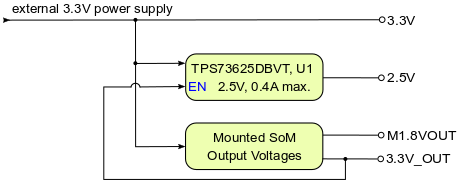
Figure 5: Board power distribution diagram.
Power Rails
The voltage direction of the power rails is from board and on-board connectors' view:
| Module Connector (B2B) Designator | VCC / VCCIO | Direction | Pins | Notes |
|---|---|---|---|---|
| JB1 | 3.3V | Out | 2, 4, 6, 14, 16 | 3.3V module supply voltage |
| VCCIOA | Out | 10, 12 | PL IO-bank VCCIO | |
| M1.8VOUT | In | 40 | 1.8V module output voltage | |
| JB2 | 3.3V_OUT | In | 9, 11 | 3.3V module output voltage |
| 3.3V | Out | 1, 3, 5, 7 | 3.3V module supply voltage | |
| VCCIOD | Out | 8, 10 | PL IO-bank VCCIO | |
| JB3 | USB-VBUS | Out | 56 | USB Host supply voltage |
Table 15: Power pin description of B2B module connector.
| On-board Pin Header Designator | VCC / VCCIO | Direction | Pins | Notes |
|---|---|---|---|---|
| J17 | 3.3V | In / Out | 5, 48 | 3.3V external supply voltage |
| VCCIOD | In / Out | 6, 45 | PL IO-bank VCCIO, depends on Jumper settings | |
| J20 | 3.3V | In / Out | 5, 48 | 3.3V external supply voltage |
| VCCIOA | In / Out | 6, 45 | PL IO-bank VCCIO, depends on Jumper settings |
Table 16: Power Pin description of on-board connector.
| Jumper / Header Designator | VCC / VCCIO | Direction | Pins | Notes |
|---|---|---|---|---|
| J26 | VCCIOA | In | 2, 4, 6 | - |
| M1.8VOUT | Out | 1 | - | |
| 2.5V | Out | 3 | - | |
| 3.3V_OUT | Out | 5 | - | |
| J27 | VCCIOD | In | 2, 4, 6 | - |
| M1.8VOUT | Out | 1 | - | |
| 2.5V | Out | 3 | - | |
| 3.3V_OUT | Out | 5 | - | |
| J4 | 3.3V | Out | 5 | - |
| M1.8VOUT | Out | 6 | - |
Table 17: Power Pin description of VCCIO selection jumper pin header.
| Peripheral Socket Designator | VCC / VCCIO | Direction | Pins | Notes |
|---|---|---|---|---|
| J10 | USB-VBUS | In | 1 | USB Host supply voltage |
Table 19: Power pin description of peripheral connector.
| XMOD Header Designator | VCC / VCCIO | Direction | Pins | Notes |
|---|---|---|---|---|
| JX1 | 3.3V | Out | 5 | connected to 3.3V external supply voltage |
| VIO | Out | 6 | ||
| J3 | 3.3V | Out | 5 | connected to 3.3V external supply voltage |
| 3.3V | Out | 6 |
Table 20: Power pin description of XMOD/JTAG Connector.
Board to Board Connectors
Unable to render {include} The included page could not be found.
Technical Specifications
Absolute Maximum Ratings
| Parameter | Min | Max | Units | Notes |
|---|---|---|---|---|
Vin supply voltage | 3.135 | 3.465 | V | 3.3V supply-voltage ± 5% |
Storage Temperature | -55 | 105 | °C | Molex 74441-0001 Product Specification |
Table 22: Board absolute maximum ratings.
Recommended Operating Conditions
| Parameter | Min | Max | Units | Notes |
|---|---|---|---|---|
| Vin supply voltage | 3.135 | 3.465 | V | - |
| Operating temperature | -40 | +85 | °C | Molex 74441-0001 Product Specification |
Table 23: Module recommended operating conditions.
Operating Temperature Ranges
Industrial grade: -40°C to +85°C.
The TEBA0841 Carrier Board itself is capable to be operated at industrial grade temperature range.
Please check the operating temperature range of the mounted SoM, which determine the relevant operating temperature range of the overall system.
Physical Dimensions
Board size: PCB 56.47 mm × 75 mm. Notice that some parts the are hanging slightly over the edge of the PCB like the mini USB-jacks and the SFP+ connector, which determine the total physical dimensions of the carrier board. Please download the assembly diagram for exact numbers.
Mating height of the module with standard connectors: 8mm
PCB thickness: ca. 1.65mm
Highest part on the PCB is the SFP+ connector, which has an approximately 11.3 mm overall hight. Please download the step model for exact numbers.
The dimensions are given in mm and mil (milli inch).
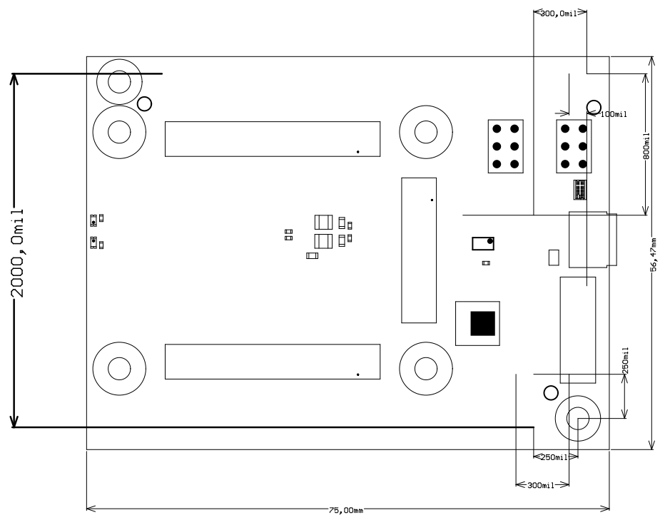
Figure 6: Board physical dimensions drawing.
Revision History
Hardware Revision History
| Date | Revision | Notes | PCN | Documentation Link |
|---|---|---|---|---|
| - | 01 |
| - | TEBA0841-01 |
Table 24: Module hardware revision history.
Hardware revision number can be found on the PCB board together with the module model number separated by the dash.
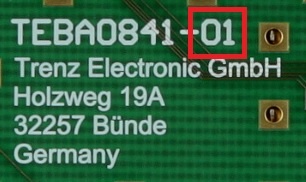
Figure 7: Board hardware revision number.
Document Change History
Date | Revision | Contributors | Description |
|---|---|---|---|
| Ali Naseri, Jan Kumann |
|
Table 25: Document change history.
Disclaimer
Data Privacy
Please also note our data protection declaration at https://www.trenz-electronic.de/en/Data-protection-Privacy
Document Warranty
The material contained in this document is provided “as is” and is subject to being changed at any time without notice. Trenz Electronic does not warrant the accuracy and completeness of the materials in this document. Further, to the maximum extent permitted by applicable law, Trenz Electronic disclaims all warranties, either express or implied, with regard to this document and any information contained herein, including but not limited to the implied warranties of merchantability, fitness for a particular purpose or non infringement of intellectual property. Trenz Electronic shall not be liable for errors or for incidental or consequential damages in connection with the furnishing, use, or performance of this document or of any information contained herein.
Limitation of Liability
In no event will Trenz Electronic, its suppliers, or other third parties mentioned in this document be liable for any damages whatsoever (including, without limitation, those resulting from lost profits, lost data or business interruption) arising out of the use, inability to use, or the results of use of this document, any documents linked to this document, or the materials or information contained at any or all such documents. If your use of the materials or information from this document results in the need for servicing, repair or correction of equipment or data, you assume all costs thereof.
Copyright Notice
No part of this manual may be reproduced in any form or by any means (including electronic storage and retrieval or translation into a foreign language) without prior agreement and written consent from Trenz Electronic.
Technology Licenses
The hardware / firmware / software described in this document are furnished under a license and may be used /modified / copied only in accordance with the terms of such license.
Environmental Protection
To confront directly with the responsibility toward the environment, the global community and eventually also oneself. Such a resolution should be integral part not only of everybody's life. Also enterprises shall be conscious of their social responsibility and contribute to the preservation of our common living space. That is why Trenz Electronic invests in the protection of our Environment.
REACH, RoHS and WEEE
REACH
Trenz Electronic is a manufacturer and a distributor of electronic products. It is therefore a so called downstream user in the sense of REACH. The products we supply to you are solely non-chemical products (goods). Moreover and under normal and reasonably foreseeable circumstances of application, the goods supplied to you shall not release any substance. For that, Trenz Electronic is obliged to neither register nor to provide safety data sheet. According to present knowledge and to best of our knowledge, no SVHC (Substances of Very High Concern) on the Candidate List are contained in our products. Furthermore, we will immediately and unsolicited inform our customers in compliance with REACH - Article 33 if any substance present in our goods (above a concentration of 0,1 % weight by weight) will be classified as SVHC by the European Chemicals Agency (ECHA).
RoHS
Trenz Electronic GmbH herewith declares that all its products are developed, manufactured and distributed RoHS compliant.
WEEE
Information for users within the European Union in accordance with Directive 2002/96/EC of the European Parliament and of the Council of 27 January 2003 on waste electrical and electronic equipment (WEEE).
Users of electrical and electronic equipment in private households are required not to dispose of waste electrical and electronic equipment as unsorted municipal waste and to collect such waste electrical and electronic equipment separately. By the 13 August 2005, Member States shall have ensured that systems are set up allowing final holders and distributors to return waste electrical and electronic equipment at least free of charge. Member States shall ensure the availability and accessibility of the necessary collection facilities. Separate collection is the precondition to ensure specific treatment and recycling of waste electrical and electronic equipment and is necessary to achieve the chosen level of protection of human health and the environment in the European Union. Consumers have to actively contribute to the success of such collection and the return of waste electrical and electronic equipment. Presence of hazardous substances in electrical and electronic equipment results in potential effects on the environment and human health. The symbol consisting of the crossed-out wheeled bin indicates separate collection for waste electrical and electronic equipment.
Trenz Electronic is registered under WEEE-Reg.-Nr. DE97922676.
Overview
Content Tools