Page History
...
| Scroll Only (inline) |
|---|
Refer to https://wiki.trenz-electronic.de/display/PD/TE0841+TRM for online version of this manual and additional technical documentation of the product. |
The Trenz Electronic TE0841-01 is an industrial-grade 4 x 5 cm SoM integrating Xilinx Kintex UltraScale FPGA, 1 GByte of DDR4 SDRAM, 32 MByte QSPI Flash for configuration and operation , and powerful switch-mode power supplies for all on-board voltages. Numerous configurable I/Os are provided via rugged high-speed strips. All this on a tiny footprint, smaller than a credit card size at very competitive price. All Trenz Electronic 4 x 5 cm SoMs are mechanically compatible.
...
Additional assembly options for cost or performance optimization plus high volume prices are available on request.
Block Diagram
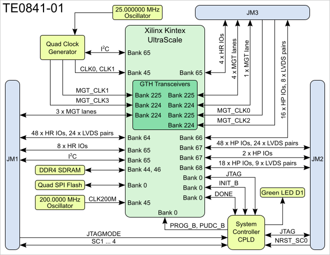
Figure 1: TE0841-01 block diagram.
...
- Xilinx Kintex UltraScale FPGA, U1
- Ultra performance oscillator @25.000000 MHz, U3
- 12A PowerSoC DC-DC converter (0.95V), U14
- 12A PowerSoC DC-DC converter (0.95V), U7
- Low-jitter precision LVDS oscillator @200.0000 MHz, U11
- Low-dropout (LDO) linear regulator (MGTAVTT 1.20V), U8
- Low-dropout (LDO) linear regulator (MGTAVCC 1.02V), U12
- Samtec Razor Beam™ LSHM-150 B2B connector, JM1
- Samtec Razor Beam™ LSHM-150 B2B connector, JM2
- Samtec Razor Beam™ LSHM-130 B2B connector, JM3
- Programmable quad clock generator, U2
- 32 MByte QSPI Flash, U6
- 4 Gbit DDR4 SDRAM, U4
- 4 Gbit DDR4 SDRAM, U5
- System Controller CPLD, U18
- Low-dropout (LDO) linear regulator (MGTAUX), U9
- Ultra-low power low-dropout (LDO) regulator (VBATT), U19
Initial Delivery State
Storage device name | Content | Notes |
|---|---|---|
| System Controller CPLD | Default firmware |
| - | ||
Quad SPI Flash OTP area | Empty | Not programmed |
| Quad clock generator OTP area | Empty | Not programmed |
Table 1: TE0841-01 module initial delivery state of programmable on-board devices.
Boot Process
By default the configuration mode pins of the FPGA are set to QSPI mode, hence the FPGA is configured from serial NOR flash at system start-up. The JTAG interface of the module is provided for configuring the QSPI flash memory with the initial FPGA configuration data.
Signals, Interfaces and Pins
...
Table below lists bank number, bank type, B2B connection, I/O signal/LVDS pair count and power source for each FPGA PL I/O bank connected to the B2B connectors:
| FPGA Bank | Type | B2B Connector | I/O Signal Count | Voltage | Notes |
|---|---|---|---|---|---|
| 64 | HR | JM1 | 48 IOs, 24 LVDS pairs | B64_VCCO | Supplied by the carrier board. |
| 65 | HR | JM1 | 8 IOs | 3.3V | On-module power supply. |
| 65 | HR | JM3 | 4 IOs, 2 LVDS pairs | 3.3V | On-module power supply. |
| 66 | HP | JM3 | 16 IOs, 8 LVDS pairs | B66_VCCO | Supplied by the carrier board |
| 67 | HP | JM2 | 48 IOs, 24 LVDS pairs | B67_VCCO | Supplied by the carrier board |
| 67 | HP | JM2 | 2 IOs | B67_VCCO | Supplied by the carrier board |
| 68 | HP | JM2 | 18 IOs, 9 LVDS pairs | B68_VCCO | Supplied by the carrier board |
...
| Clock signal | Bank | Source | FPGA Pin | Notes |
|---|---|---|---|---|
| MGT_CLK0_P | 225 | B2B, JM3-33 | MGTREFCLK0P_225, Y6 | Supplied by the carrier board. |
| MGT_CLK0_N | 225 | B2B, JM3-31 | MGTREFCLK0N_225, Y5Supplied by the carrier board. | |
| MGT_CLK1_P | 225 | U2, CLK1B | MGTREFCLK1P_225, V6 | On-board Si5338A. |
| MGT_CLK1_N225 | U2, CLK1A | MGTREFCLK1N_225, V5On-board Si5338A. | ||
| MGT_CLK2_P | 224 | B2B, JM3-34 | MGTREFCLK2P_224, AD6 | Supplied by the carrier board. |
| MGT_CLK2_N | 224 | B2B, JM3-32 | MGTREFCLK2N_224, AD5 | Supplied by the carrier board. |
| MGT_CLK3_P | 224 | U2, CLK2B | MGTREFCLK3P_224, AB6 | On-board Si5338A. |
| MGT_CLK3_N224 | U2, CLK2B | MGTREFCLK3N_224, AB5On-board Si5338A. |
Table 4: MGT banks reference clock sources.
...
| Note |
|---|
| JTAGMODE pin 89 in B2B connector JM1 should be set low or grounded for normal operation. Set this high for SC CPLD update vie JTAG interface. |
| Page break |
|---|
System Controller CPLD I/O Pins
...
| Pin Name | Mode | Function | Default Configuration |
|---|---|---|---|
| JTAGMODE | Input | JTAG select | Low for normal operation. |
| NRST_SC0 | Input | Reset | - |
| SC1 | - | - | Not used by default. |
| SC2 | - | - | Not used by default. |
| SC3 | - | - | Not used by default. |
| SC4 | - | - | Not used by default. |
...
Quad SPI interface is connected to the FPGA configuration bank 0.
| Signal Name | QSPI Flash Memory U6 Pin | FPGA Pin |
|---|---|---|
| SPI_CS | C2 | RDWR_FCS_B_0, AH7 |
| SPI_D0 | D3 | D00_MOSI_0, AA7 |
| SPI_D1 | D2 | D01_DIN_0, Y7 |
| SPI_D2 | C4 | D02_0, U7 |
| SPI_D3 | D4 | D03_0, V7 |
| SPI_CLK | B2 | CCLK_0, V11 |
...
There is a Silicon Labs I2C programmable quad PLL clock generator on-board (Si5338A, U2) to generate various several reference clocks for the module.
| Si5338A Pin | Signal Name / Description | Connected To | Direction | Note | |
|---|---|---|---|---|---|
IN1 | - | Not connected. | Input | Not used. | |
| IN2 | - | GND | Input | Not used. | |
IN3 | Reference input clock. | U3, pin 3 | Input | 25.000000 MHz oscillator, Si8208AI. | |
IN4 | - | GND | Input | I2C slave device address LSB. | |
IN5 | - | Not connected. | Input | Not used. | |
| IN6 | - | GND | Input | Not used. | |
CLK0A | CLK1_P | U1, R23 | Output | FPGA bank 45. | |
| CLK0B | CLK1_N | U1, P23 | OutputFPGA bank 45. | ||
| CLK1A | MGT_CLK1_N | U1, V5 | Output | FPGA MGT bank 225 reference clock. | |
| CLK1B | MGT_CLK1_P | U1, V6 | Output | V6 | OutputFPGA MGT bank 225 reference clock. |
| CLK2A | MGT_CLK3_N | U1, AB5 | Output | FPGA MGT bank 224 reference clock. | |
| CLK2B | MGT_CLK3_P | U1, AB6 | Output | FPGA MGT bank 224 reference clock. | |
| CLK3A | CLK0_P | U1, pin T24 | Output | FPGA bank 45. | |
| CLK3B | CLK0_N | U1, pin T25 | OutputFPGA bank 45. |
Table 8: Programmable quad PLL clock generator inputs and outputs.
...
| Clock Source | Frequency | Signal Name | Clock Destination | ||
|---|---|---|---|---|---|
| U3, SiT8208AI | 25.000000 MHz | CLK | U2, pin 3 (IN3) | ||
| U11, DSC1123DL5 | 200.0000 MHz | CLK200M_P | U1, pin R25 | U11, DSC1123DL5 | 200.0000 MHz |
| CLK200M_N | U1, pin R26 | ||||
| B2B, JM3-31 | User | MGT_CLK0_N | U1, pin Y5 | ||
| B2B, JM3-33User | MGT_CLK0_P | U1, pin Y6 | |||
| B2B, JM3-32 | User | MGT_CLK2_N | U1, pin AD5 | ||
| B2B, JM3-34User | MGT_CLK2_P | U1, pin AD6 |
Table 9: Reference clock signals.
...
See also Xilinx datasheet DS892 for additional information. User should also check related baseboard documentation when choosing baseboard design for TE0841 module.
| Page break |
|---|
Power Rails
| Power Rail Name | B2B JM1 Pins | B2B JM2 Pins | Input/Output | Notes |
|---|---|---|---|---|
| VIN | 1, 3, 5 | 2, 4, 6, 8 | Input | Supply voltage. |
| 3.3VIN | 13, 15 | - | Input | Supply voltage. |
| B64_VCO | 9, 11 | - | Input | HR (High Range) bank voltage. |
| B66_VCO | - | 1, 3 | Input | HP (High Performance) bank voltage. |
| B67_VCO | - | 7, 9 | Input | HP (High Performance) bank voltage. |
| B68_VCO | - | 5 | Input | HP (High Performance) bank voltage. |
VBAT_IN | 79 | - | Input | RTC battery supply voltage. |
| 3.3V | - | 10, 12, 91 | Output | Module on-board 3.3V voltage level. |
Table 12: Module power rails.
...
Variants Currently In Production
| Module Variant | FPGA Chip | Temperature Range |
|---|---|---|
| TE0841-01-035-1C | XCKU035-1SFVA784C | Commercial |
TE0841-01-035-1I | XCKU035-1SFVA784I | Industrial |
TE0841-01-035-2I | XCKU035-2SFVA784I | Industrial |
| TE0841-01-040-1C | XCKU040-1SFVA784C | Commercial |
| TE0841-01-040-1I | XCKU040-1SFVA784I | Industrial |
Table 13: Module variants in production.
Technical Specifications
Absolute Maximum Ratings
Parameter | Min | Max | Units | Reference Document |
|---|---|---|---|---|
VIN supply voltage | -0.3 |
| 6.0 | V | EN63A0QI, |
| TPS74401RGW datasheets. | ||||
| 3.3VIN supply voltage | -0.1 | 3.75 | V | TPS27082, LCMXO2-256HC datasheets. |
| Supply voltage for HR I/O banks (VCCO) |
-0.500 | 3.400 | V | Xilinx datasheet DS892. |
Supply voltage for HP I/O banks (VCCO) |
-0.500 | 2.000 | V | Xilinx datasheet DS892. |
| I/O input voltage for HR I/O banks |
-0.400 | VCCO + 0.550 | V | Xilinx datasheet DS892. |
I/O input voltage for HP I/O banks |
-0.550 | VCCO + 0.550 | V | Xilinx datasheet DS892. | |
| GTH and GTY transceiver reference clocks absolute input voltage (MGT_CLK0, MGT_CLK2) | -0.500 | 1.320 | V | Xilinx datasheet DS892. |
GTH and GTY transceiver receiver (RXP/RXN) and transmitter (TXP/TXN) absolute input voltage | -0.500 | 1.260 | V | Xilinx datasheet DS892. |
Storage temperature | -40 | +85 | °C | - |
Table 14: Module absolute maximum ratings.
Recommended Operating Conditions
| Parameter | Min | Max | Units | Reference Document |
|---|---|---|---|---|
| VIN supply voltage |
| 3.3 | 5 |
| . |
| 5 | V | TPS82085SIL, TPS74401RGW datasheet |
| 3.3VIN supply voltage | 2.375 | 3.6 | V | LCMXO2-256HC datasheet |
| Supply voltage for HR I/O banks (VCCO) | 1.140 | 3.400 | V | Xilinx datasheet DS892 |
Supply voltage for HP I/O banks (VCCO) | 0.950 | 1.890 | V | Xilinx datasheet DS892 |
I/O input voltage | –0.200 | VCCO + 0.20 | V | Xilinx datasheet DS892 |
Table 15: Module recommended operating conditions.
...
Hardware Revision History
| Date | Revision | Notes | PCN | Documentation Link |
|---|---|---|---|---|
| 2015-12-09 | 01 | First production revision | - | TE0841-01 |
Table 16: Hardware revision history.
...
Date | Revision | Contributors | Description | ||||||||
|---|---|---|---|---|---|---|---|---|---|---|---|
| Jan Kumann, Ali Naseri | Initial document. |
Table 17: Document change history.
...
Overview
Content Tools