Page History
| Scroll Ignore |
|---|
Download PDF version of this document. |
| Scroll pdf ignore | |
|---|---|
Table of Contents
|
Overview
| Scroll Only (inline) |
|---|
Refer to https://shop.trenz-electronic.de/de/Download/?path=Trenz_Electronic/carrier_boards/TE0703 for downloadable version of this manual and the rest of available documentation. |
The Trenz Electronic TE0703 Carrier Board is a base-board for 4x5 SoM's, which exposes the MIO- and the PS/PL-pins of the SoM to accessible connectors and provides a whole range of on-board-components to test and evaluate Trenz Electronic 4x5 SoM's.
See page "4 x 5 cm carriers" to get information about the SoM's supported by the TE0703 Carrier Board.
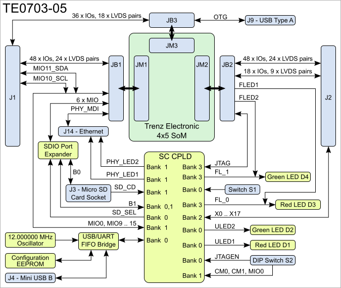
Block Diagram
Main Components
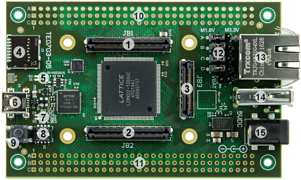
- Samtec Razor Beam™ LSHM-150 B2B connector, JB1
- Samtec Razor Beam™ LSHM-150 B2B connector, JB2
- Samtec Razor Beam™ LSHM-130 B2B connector, JB3
- Micro SD card socket with detect switch, J3
- LED indicators D1 and D2
- Mini-USB type B connector, J4
- LED indicators D3 and D4
- Configuration DIP switches, S2 (see table under "DIP switches" section)
- User push button (Reset), S1
- External connector (VG96) placeholder, J1
- External connector (VG96) placeholder, J2
- VCCIO voltage selection jumper block, J5, J8, J9 and J10 (see "Power and Power-On Sequence" section)
- Trxcom 1000Base-T Gigabit RJ45 Magjack, J14
- USB type A receptacle, J6 (optional micro USB 2.0 type B receptacle available, J12)
- 5V power connector jack, J13
Key Features
- 2 x VG96 backplane connectors (mounting holes and solder pads)
- SDIO port expander with voltage-level translation
- Micro SD card socket, can be used to boot system
- 4 x user LED's, 2 x red and 2 x green
- Mini-USB connector (USB JTAG and UART interface)
- 1 x user push-button routed to CPLD. By default it is configured as system reset button
- RJ45 Gigabit Ethernet socket with 4 integrated LED's
- USB Host Connector
- Barrel jack for 5V power supply input
- 4A high-efficiency power SoC DC-DC step-down converter(Enpirion EN6347) for 3.3V power supply
- Trenz 4x5 module connector strips (3 x Samtec LSHM series connectors)
- USB JTAG and UART interface (FTDI FT2232H), compatible with Xilinx Tools (also with many other tools)
- 2 x user configurable DIP switches
Initial Delivery State
Board is shipped in following configuration:
- VCCIO voltage selection jumpers are all set to 1.8 V.
- S1 switch configured as reset button in CPLD.
- Two VG96 backplane connectors are not soldered to the board, but they are included in the package as separate components.
- S2 DIP switches are configured as follows:
| Switch | Position | Description |
|---|---|---|
| S2-1 | ON | Mode control MC1. |
| S2-2 | ON | FPGA access on module (need also S2-3 ON) |
S2-3 | ON | FPGA access on module (need also S2-2 ON) |
| S2-4 | OFF | Boot mode set to QSPI. |
Different delivery configurations are available upon request.
Signals, Interfaces and Pins
Board to Board (B2B) I/O's
For detailed information about the B2B pin out, please refer to the Master Pin-out Table.
Micro SD Card Socket
Micro SD card socket is connected to the B2B connector through a Texas Instruments TXS02612 SDIO port expander for voltage translation. The Micro SD card has 3.3V signal voltage level while most 4x5 modules use 1.8V for the SD card interface.
USB JTAG and UART
TE0703 has on-board USB JTAG and UART solution based on UART/FIFO controller from FTDI. FTDI EEPROM is pre-programmed with license code to support Xilinx programming tools.
| Warning |
|---|
Do not access the FT2232H EEPROM using FTDI programming tools, doing so will erase normally invisible user EEPROM content and invalidate stored Xilinx JTAG license. Without this license the on-board JTAG will not be accessible any more with any Xilinx tools. Software tools from FTDI website do not warn or ask for confirmation before erasing user EEPROM content. |
Ethernet
On-board Ethernet jack J14 pins are routed to B2B connector JB1. Ethernet jack J14 LEDs PHY_LED1 and PHY_LED2 are both routed to System Controller CPLD bank 1.
USB Interface
TE0703 board has two physical USB sockets:
- J4 as mini-USB type B socket wired to the on-board FTDI FT2232H chip.
- J6 as USB type A wired to B2B connector JB3 (USB transceiver used depends on the SoM model used).
| Page break |
|---|
JTAG Interface
JTAG access to the System Controller CPLD and Xilinx Zynq chip on the SoM is provided via mini-USB JTAG interface (FTDI FT2232H) and controlled by DIP switch S2-3. JTAG signals from System Controller CPLD to the JB2 connector are routed as follows:
JTAG Signal | B2B Connector Pin |
|---|---|
| TCK | JB2-100 |
| TDO | JB2-98 |
| TDI | JB2-96 |
| TMS | JB2-94 |
LEDs
There are four on-board LEDs:
| LED | Color | Description |
|---|---|---|
| D1 | Red | FTDI UART receive activity. |
| D2 | Green | FTDI UART transmit activity. |
| D3 | Red | CPLD signal FL_0. |
| D4 | Green | CPLD signal FL_1. |
LEDs D3 and D4 are also connected to the B2B connector JB2 pins FLED1 and FLED2 respectively and can be controlled by SoM FPGA firmware.
DIP switches
DIP switch settings are CPLD Firmware depends, default firmware:
| Switch | ON | OFF | Notes |
|---|---|---|---|
| S2-1 | Force CD Pin to module to GND | set CD Pin to module to SD CD Pin | TE0703 CPLD - CC703S#CC703S-SD |
| S2-2 | Module FPGA JTAG access ( if S2-3 ON) | Module CPLD JTAG access ( if S2-3 ON) | TE0703 CPLD - CC703S#CC703S-JTAG |
| S2-3 | Module FPGA/CPLD JTAG access ( depends on S2-3) | Carrier CPLD JTAG access | TE0703 CPLD - CC703S#CC703S-JTAG |
| S2-4 | Boot from SD Card (set Pin to GND) | Boot from QSPI flash on module (set Pin to VDD) | TE0703 CPLD - CC703S#CC703S-BootMode |
Mode status is displayed on TE0703 LEDs, see TE0703 CPLD - CC703S#CC703S-LED.
Power
Power supply with minimum current capability of 3A for system startup is recommended.
Power Supply
Single power supply with minimum current capability of 3A at 5V for system startup is recommended.
Power Consumption
| Power Input Pin | Max Current |
|---|---|
| VIN (power connector jack J13) | 4A |
Typical power consumption for TE0703-05 + TE0715-01 module with SD micro card inserted, Ethernet connected and link up, system booted into Linux prompt and idling is 5V / 0.55A.
Power-On Sequence
It is not allowed to feed any voltage to any external I/O pin before there is no power indication on M3.3VOUT pins. Presence of 3.3V on B2B JB2 connector pins 9 and 11 indicates that module is properly powered up and ready.
If any of the VCCIOA, VCCIOB, VCCIOC or VCCIOD will be powered through external connectors J1 or J2, then corresponding VCCIO jumper should also be removed altogether, see next chapter.
VCCIO voltage selection jumpers J5, J8, J9 and J10
Refer to the 4x5 Module Integration Guide for VCCIO voltages options.
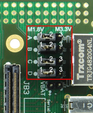
Jumper J5 | 1-2 | 2-3 | Voltage |
|---|---|---|---|
VCCIOA | ON | OFF | 1.8 V |
| VCCIOA | OFF | ON | 3.3 V |
| Jumper J8 | 1-2 | 2-3 | Voltage |
|---|---|---|---|
| VCCIOB | ON | OFF | 1.8 V |
| VCCIOB | OFF | ON | 3.3 V |
| Jumper J9 | 1-2 | 2-3 | Voltage |
|---|---|---|---|
| VCCIOC | ON | OFF | 1.8 V |
| VCCIOC | OFF | ON | 3.3 V |
| Jumper J10 | 1-2 | 2-3 | Voltage |
|---|---|---|---|
| VCCIOD | ON | OFF | 1.8 V |
| VCCIOD | OFF | ON | 3.3 V |
| Note |
|---|
Take care of the VCCO voltage ranges of the particular PL IO-banks (HR, HP) of the mounted SoM, otherwise damages may occur to the FPGA. Therefore, refer to the TRM of the mounted SoM to get the specific information of the voltage ranges. It is recommended to set and measure the PL IO-bank supply-voltages before mounting of TE 4 x 5 module to avoid failures and damages to the functionality of the mounted SoM. |
Board to Board Connectors
| Include Page | ||||
|---|---|---|---|---|
|
Technical Specifications
Absolute Maximum Ratings
Parameter | Min | Max | Units | Reference document |
|---|---|---|---|---|
Supply Voltage VCC | -0.33 | 5.5 | V | |
| Operating temperature | -40 | +125 | °C | Lattice Semiconductor MachXO2 family datasheet |
Storage temperature | -55 | +125 | °C |
Recommended Operating Conditions
Parameter | Min | Max | Units | Reference document |
|---|---|---|---|---|
Supply voltage VCC | 4.75 | 5.25 | V | |
| Operating temperature | 0 | +70 | °C |
| Note |
|---|
| Assembly variants for higher storage temperature range are available on request. |
| Note |
|---|
| Please check components datasheets for complete list of absolute maximum and recommended operating ratings. |
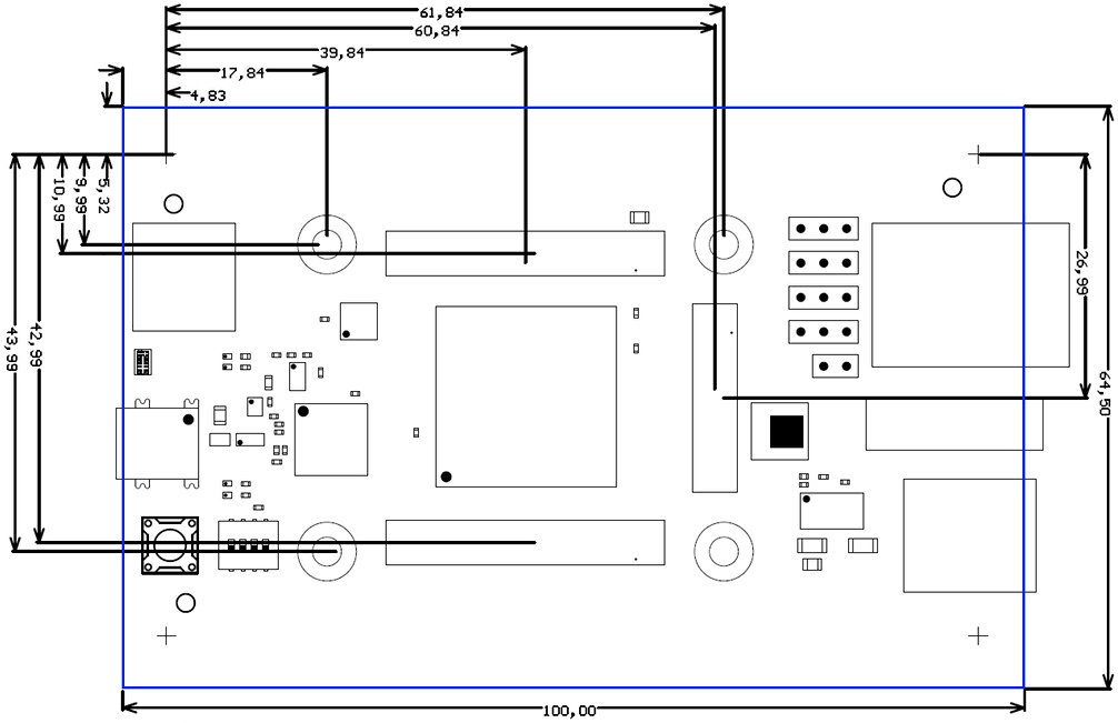
Physical Dimensions
Board size: 100 mm × 64.5 mm. Notice that the mini-USB jack on the left and ethernet RJ-45 jack on the right are hanging slightly over the edge of the PCB making the total width of the longer side approximately 106 mm. Please download the assembly diagram for exact numbers.
Mating height of the module with standard connectors: 8 mm
PCB thickness: 1.65 mm
Highest parts on the PCB are USB type A jack and ethernet RJ-45 jack, approximately 15 mm. Please download the step model for exact numbers.
All dimensions are given in millimeters.
Operating Temperature Ranges
Commercial grade: 0°C to +70°C.
Industrial grade: -40°C to +85°C.
Board operating temperature range depends also on customer design and cooling solution. Please contact us for options.
Weight
42g - Plain board.
13g - 2 x VG96 connectors.
Revision History
Hardware Revision History
Date | Revision | Notes | PCN | Documents |
|---|---|---|---|---|
2016-09-07 | 05 | Added VCCIO Jumpers | TE0703 | |
- | 04 | Corrected FTDI EEPROM connection | - | TE0703-04 |
- | 03 | Added VCCIO strapping resistors | - | |
- | 02 | First series boards | - | |
- | 01 | Prototypes | - |
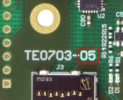
Hardware revision number is printed on the PCB board next to the module model number separated by the dash.
Document Change History
Date | Revision | Contributors | Description | ||||||||
|---|---|---|---|---|---|---|---|---|---|---|---|
| John Hartfiel |
| |||||||||
| 2017-11-09 | v.26 | John Hartfiel |
| ||||||||
| 2017-02-21 | v.19 | Jan Kumann |
| ||||||||
| 2017-02-02 | v.16 | Jan Kumann |
| ||||||||
| 2016-12-22 | v.14 | Jan Kumann |
| ||||||||
| 2016-12-08 | v.10 | Jan Kumann |
| ||||||||
| 2016-12-05 | v.5 | John Hartfiel |
| ||||||||
| 2016-09-06 | v.1 | Jan Kumann, John Hartfiel |
|
Disclaimer
| Include Page | ||||
|---|---|---|---|---|
|
Overview
Content Tools