Page History
...
| Function | MGT Lane | Schematic Names / B2B pins | Required Ref Clock | Clock Source | Comment |
|---|---|---|---|---|---|
| PCIe | PS 0 | PCI_TX_N, pin J2-67 PCI_RX_N, pin J2-70 | 100 MHz | clock signal of SoM's prog. PLL | single lane PCIe connector clock signal routed on carrier board to PCIe connector J1 |
| USB3 | PS 1 | USB3_TXUP_N, pin J2-61 USB3_RXUP_N, pin J2-64 | 100 MHz | clock signal of SoM's prog. PLL | clock signal routed on-module, |
| SATA | PS 2 | SATA_TX_N, pin J2-55 SATA_RX_N, pin J2-58 | 150 MHz | On-board oscillator U23 | optional: clock signal of SoM's prog. PLL |
| DP.0 | PS 3 | DP0_TX_N, pin J2-49 | 27 MHz | clock signal of SoM's prog. PLL | DisplayPort GT SERDES clock signal, |
...
Following diagram visualizes the connection of the DC-DC converter control signals ('Enable', 'Power-Good') with System Controller CPLD U39, which enables the particular on-board voltages.
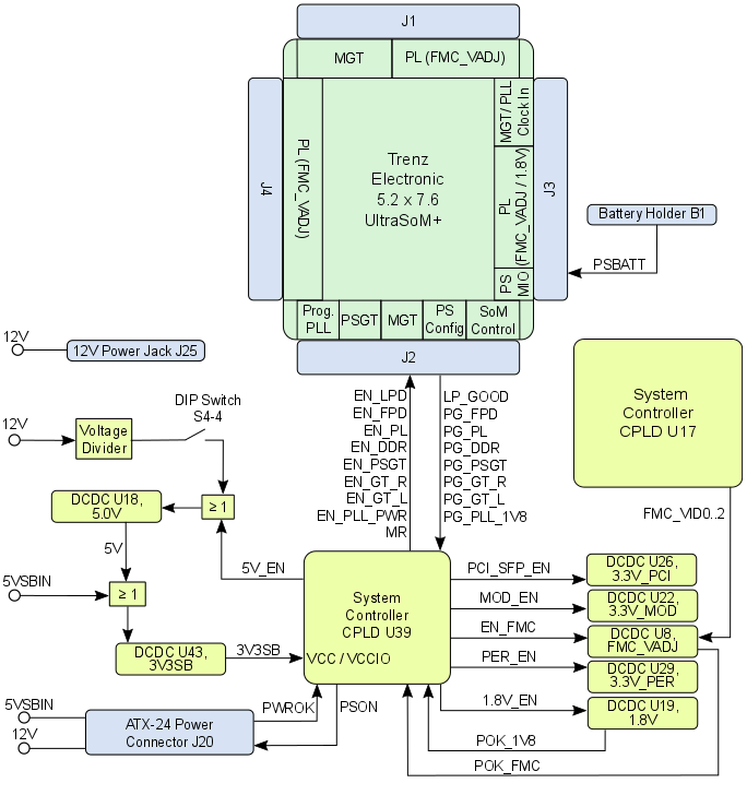
Figure 13: Power-On Sequence Utilizing DCDC Converter Control Signals
...
| Date | Revision | Contributors | Description | ||||||||
|---|---|---|---|---|---|---|---|---|---|---|---|
| John Hartfiel |
| |||||||||
| 2017-11-15 | v.86 | Ali Naseri |
| ||||||||
2017-11-13 | v.82 | Ali Naseri |
| ||||||||
2017-11-13 | v.80 | John Hartfiel |
| ||||||||
| 2017-10-19 | v.79 | Ali Naseri |
| ||||||||
2017-10-18 | v.75 | Ali Naseri |
| ||||||||
2017-08-29 | v.70 | John Hartfiel |
| ||||||||
| 2017-08-28 | v.69 | Ali Naseri |
|
...
Overview
Content Tools