Page History
...
| HTML |
|---|
<!-- General Design description --> |
Zynq PS Design with Linux Example. Add simple frequency counter to measure SI5338 Reference CLK and RGPIO IP to get access to CPLD IOs with Vivado HW-Manager.
Key Features
| HTML |
|---|
<!-- Add Basic Key Features of the design (should be tested) --> |
| Excerpt |
|---|
|
...
| HTML |
|---|
<!-- - Add changes from design - Export PDF to download, if vivado revision is changed! --> |
| Date | Vivado | Project Built | Authors | Description |
|---|---|---|---|---|
| 2018-06-01 | 2017.4 |
Release Notes and Know Issues
| TE0783-test_board_noprebuilt-vivado_2017.4-build_10_20180611114036.zip TE0783-test_board-vivado_2017.4-build_10_20180611114017.zip | John Hartfiel | initial release |
Release Notes and Know Issues
| HTML |
|---|
<!--
- add |
| HTML |
<!--
- add known Design issues and general Notes for the current revision
--> |
...
- Open Serial Console (e.g. putty)
- Speed: 115200
- COM Port: Win OS, see device manager, Linux OS see dmesg |grep tty (UART is *USB1)
- Linux Console:
Note: Wait until Linux boot finished For Linux Login use:- User Name: root
- Password: root
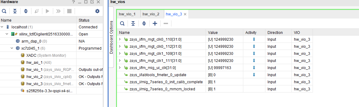
Vivado HW Manager
SI5338 MGT Reference CLKs:
- You can use Linux shell now.
- I2C 0 Bus type: i2cdetect -y -r 0
- RTC check: dmesg | grep rtc
- ETH0 works with udhcpc
- USB type "lsusb" or connect USB2.0 device
Vivado HW Manager
SI5338 MGT Reference CLKs:
- Open Vivado HW-Manager Open Vivado HW-Manager and add VIO signal to dashboard (*.ltx located on prebuilt folder).
- Set radix from VIO signals to unsigned integer.
Note: Frequency Counter is inaccurate and displayed unit is Hz - SI5338 CLK is CLKs are configured to to 125MHz with example FSBL initialisation.
PL MIG Status Signals
TODO Bild
System Design - Vivado
Status signal:
- Status signals connected to VIO
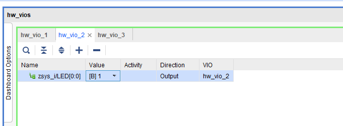
Custom LED
Red LED D1 can be controlled via VIO.
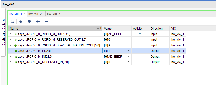
RGPIO
RGPIO Pins can be controlled via VIO
System Design - Vivado
| HTML |
|---|
<!-- |
| HTML |
<!--
Description of Block Design, Constrains...
BD Pictures from Export...
--> |
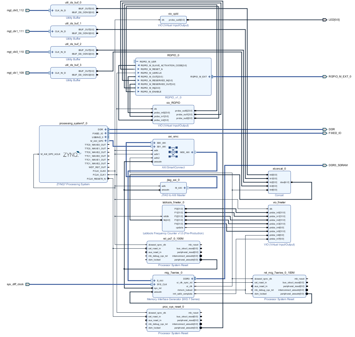
Block Design
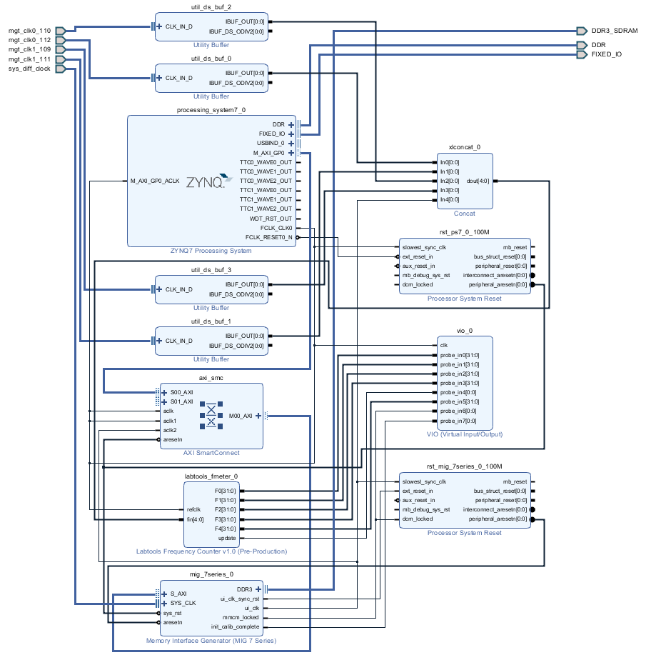
PS Interfaces
| Typ | Note |
|---|---|
| DDR3 | |
| QSPI | MIO |
| ETH0 | MIO |
| USB0 | MIO |
| SD0 | MIO |
| SD1 | MIO |
| I2C0 | MIO |
| SWDT0..1 | |
| TTC0..3 |
Constrains
Basic module constrains
| Code Block | ||||
|---|---|---|---|---|
| ||||
set_property BITSTREAM.GENERAL.COMPRESS TRUE [current_design]
set_property CONFIG_VOLTAGE 3.3 [current_design]
set_property CFGBVS VCCO [current_design] |
Design specific constrain
_design]
set_property CONFIG_VOLTAGE 3.3 [current_design]
set_property CFGBVS VCCO [current_design] |
Design specific constrain
| Code Block | ||||
|---|---|---|---|---|
| ||||
#set_property PACKAGE_PIN AA8 [get_ports {SI_MGT_CLK0_110_clk_p[0]}]
#set_property PACKAGE_PIN N8 [get_ports {SI_MGT_CLK0_112_clk_p[0]}]
#set_property PACKAGE_PIN AF10 [get_ports {SI_MGT_CLK1_109_clk_p[0]}]
#set_property PACKAGE_PIN W8 [get_ports {SI_MGT_CLK1_111_clk_p[0]}]
#set_property IOSTANDARD DIFF_SSTL15 [get_ports {MIG_SYS_CLK_clk_p[0]}]
#set_property PACKAGE_PIN H9 [get_ports {MIG_SYS_CLK_clk_p[0]}]
# -------------
#LED
set_property PACKAGE_PIN AE20 [get_ports {LED[0]}]
set_property IOSTANDARD LVCMOS33 [get_ports {LED[0]}]
# -------------
#RGPIO
set_property PACKAGE_PIN AB19 [get_ports RGPIO_M_EXT_0_clk]
set_property PACKAGE_PIN AB20 [get_ports RGPIO_M_EXT_0_rx]
set_property PACKAGE_PIN AD20 [get_ports RGPIO_M_EXT_0_tx]
set_property IOSTANDARD LVCMOS33 [get_ports RGPIO_M_EXT_0_clk]
set_property IOSTANDARD LVCMOS33 [get_ports RGPIO_M_EXT_0_rx]
set_property IOSTANDARD LVCMOS33 [get_ports RGPIO_M_EXT_0_tx] |
| Code Block | ||||
|---|---|---|---|---|
| ||||
set_false_path -from [get_clocks clk_fpga_0] -to [get_clocks {zsys_i/util_ds_buf_0/U0/IBUF_OUT[0]}]
set_false_path -from [get_clocks clk_fpga_0] -to [get_clocks {zsys_i/util_ds_buf_1/U0/IBUF_OUT[0]}]
set_false_path -from [get_clocks clk_fpga_0] -to [get_clocks {zsys_i/util_ds_buf_2/U0/IBUF_OUT[0]}]
set_false_path -from [get_clocks clk_fpga_0] -to [get_clocks {zsys_i/util_ds_buf_3/U0/IBUF_OUT[0]}]
set_false_path -from [get_clocks {zsys_i/util_ds_buf_0/U0/IBUF_OUT[0]}] -to [get_clocks clk_fpga_0]
set_false_path -from [get_clocks {zsys_i/util_ds_buf_1/U0/IBUF_OUT[0]}] -to [get_clocks clk_fpga_0]
set_false_path -from [get_clocks {zsys_i/util_ds_buf_2/U0/IBUF_OUT[0]}] -to [get_clocks clk_fpga_0]
set_false_path -from [get_clocks {zsys_i/util_ds_buf_3/U0/IBUF_OUT[0]}] -to [get_clocks clk_fpga_0] | ||||
| Code Block | ||||
| language | ruby | title | _i_io.xdc
Software Design - SDK/HSI
...
| Date | Document Revision | Authors | Description | ||||||||||||||||||||||
|---|---|---|---|---|---|---|---|---|---|---|---|---|---|---|---|---|---|---|---|---|---|---|---|---|---|
|
|
| Work in progress
| ||||||||||||||||||||||
| 2018-05-30 | v.1 |
|
| ||||||||||||||||||||||
| All |
|
...
Overview
Content Tools