Page History
| HTML |
|---|
<!-- Template Revision 1.6468 (HTML comments will be not displayed in the document, no need to remove them. For Template/Skeleton changes, increase Template Revision number. So we can check faster, if the TRM style is up to date). --> |
...
| HTML |
|---|
<!-- General Notes: Designate all graphics and pictures with a number and a description. For example "Figure 1: TE07xx-xx Block Diagram" or "Table 1: Initial delivery state". "Figure x" and "Table x" have to be formatted to bold. --> |
| HTML |
|---|
<!-- Download Link: Goto tothe Basebase Folderfolder of the Module module (remove de/ or Carrier,en/ from the URL): for example : https://shop.trenz-electronic.de/en/Download/?path=Trenz_Electronic/TE0712 Use english URL "../en/.. /Modules_and_Module_Carriers/4x5/4x5_Carriers/TE0703/ --> |
| Scroll Ignore |
|---|
| Scroll pdf ignore | |
|---|---|
Table of Contents
|
Overview
| HTML |
|---|
<!--
Wiki Link: Go to Base Folder of the Module or Carrier, for example : https://wiki.trenz-electronic.de/display/PD/TE0706
--> |
| Scroll Only (inline) |
|---|
Refer to https://wiki.trenz-electronic.de/display/PD/TEBA0841+TRM for the current online version of this manual and other available documentation.
|
The Trenz Electronic TEBA0841 is a Carrier Board for testing, evaluation and development purposes, especially for the Multi-gigabit transceiver units of the TE0841 and TE0741 modules. Although this base-board is dedicated to the modules TE0841 and TE0741, it is also compatible with other Trenz Electronic 4 x 5 cm SoMs.
...
The Trenz Electronic TEBA0841 is a low cost carrier board for testing, evaluation and development purposes of the TE0841 and TE0741 modules. Although this base-board is dedicated to the modules TE0841 and TE0741, it is also compatible with other Trenz Electronic 4 x 5 cm SoMs. The carrier board offers one SFP connector, one Micro USB2 B connector, two 2x25-pin headers and one XMOD header to get access to the I/O's and interfaces of FPGA modules. To test and evaluate the Multi-gigabit transceiver units of the FPGA module, 6 MGT lanes on the carrier board are routed in a loop-back circuit on the B2B connectors.
See page "4 x 5 cm carriers" to get information about the SoMs supported by the TEBA0841 carrier board.
| HTML |
|---|
<!--
Use short link the Wiki Ressource page: for example:
http://trenz.org/te0720-info
List of available short links: https://wiki.trenz-electronic.de/display/CON/Redirects
--> |
| Scroll Only (inline) |
|---|
Refer to http://trenz.org//teba0841-info for the current online version of this manual and other available documentation. |
Key Features
- SFP+ connector (Enhanced small form-factor pluggable), supports data transmission rates up to 10 Gbit/s
- Micro USB2 .0 Type B Connector (J10)
- Trenz Electronic 4x5 module Socket B2B connectors (3 x Samtec LSHM series connectors)
- 4 x 5 SoM programmable by XMOD JTAG/UART header (JX1)
- 2 x user LEDs routed to I/O-pins of the SoM
- Soldering-pads J17 and J20 for optional pin headers for access to SoM's I/O-bank - pins, usable as LVDS-pairs
- Soldering-pads J3 and J4 for optional pin headers for access to further interfaces and I/O's of the SoM
- 2 x user LEDs routed to I/O-pins of the SoM
- 4-bit DIP switch for setting module parameters
- 4x VCCIO selection jumper to set module's bank voltages
Additional assembly options are available for Additional assembly options are available for cost or performance optimization upon request.
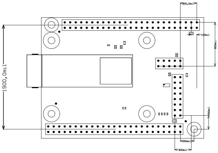
Block Diagram
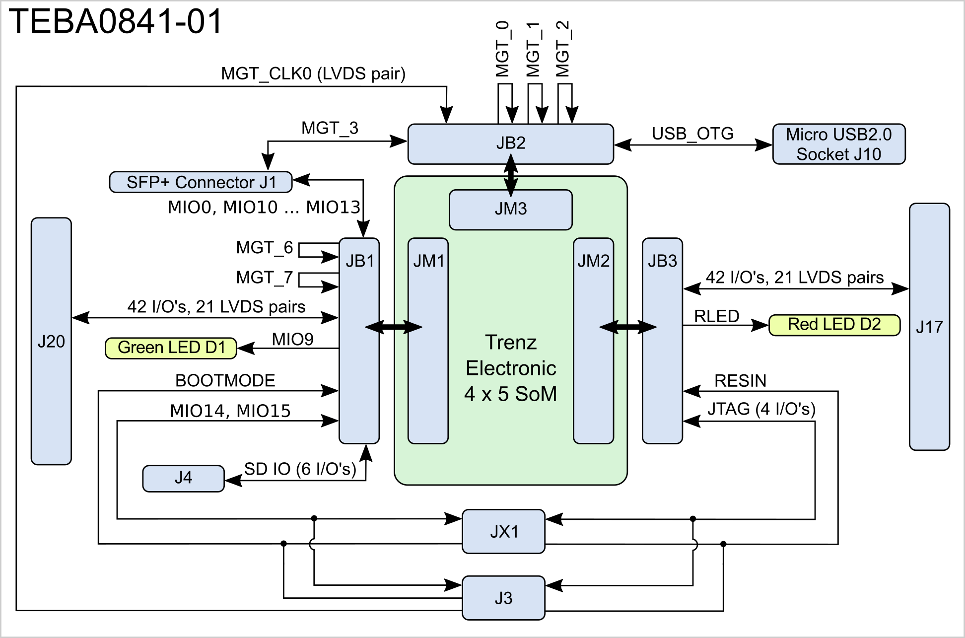
Figure 1: TEBA0841-01 Block Diagram.
Main Components
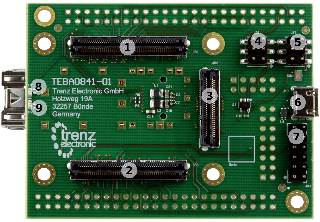
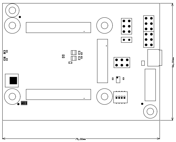
Figure 2: TEBA0841-01 Carrier Board.
| HTML |
|---|
<!--
Rules for all diagrams:
1. All diagrams are wrapped in the "Scroll Title" macro.
	- The title has to be named with the diagrams name
	- The anchor has the designation figure_x, whereby x is the number of the diagram

2. The Draw.IO diagram has to be inserted in the "Scroll Ignore" macro
	- Border has to be switched off in the macro edit
	- Toolbar has to be hidden in the macro edit

3. A PNG Export of the diagram has to be inserted in the "Scroll Only" macro, see Wiki page "Diagram Drawing Guidelines" how to do this step.

The workaround with the additional PNG of the diagram is necessary until the bug of the Scroll PDF Exporter, which cuts diagram to two pages, is fixed.


IMPORTANT NOTE: In case of copy and paste the TRM skeleton to a new Wiki page, delete the Draw.IO diagrams and the PNGs, otherwise due to the linkage of the copied diagrams every change in the TRM Skeleton will effect also in the created TRM and vice versa!

See page "Diagram Drawing Guidelines" how to clone an existing diagram as suitable template for the new diagram!


--> |
| Scroll Title | ||||||||||||||||||||||||
|---|---|---|---|---|---|---|---|---|---|---|---|---|---|---|---|---|---|---|---|---|---|---|---|---|
| ||||||||||||||||||||||||
|
Main Component
| Scroll Title | ||||||||||||||||||||||||
|---|---|---|---|---|---|---|---|---|---|---|---|---|---|---|---|---|---|---|---|---|---|---|---|---|
| ||||||||||||||||||||||||
|
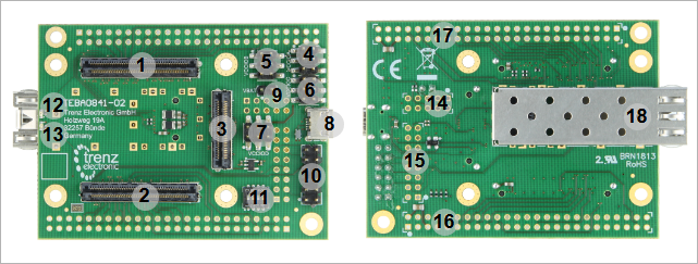
Photo shows similar TEBA0841-01
- Samtec Razor Samtec Razor Beam™ LSHM-150 B2B connector, JB1
- Samtec Razor Beam™ LSHM-150 B2B connector, JB3
- Samtec Razor Beam™ LSHM-130 B2B connector, JB2
- 6-pin header J26, for selecting PL I/O-bank voltage
- 6-pin header J27, for selecting PL I/O-bank voltage
- Micro USB2 .0 Type B Connector connector J12 (Device or OTG mode)
- XMOD FTDI JTAG/UART header, JX1 ('XMOD FTDI JTAG Adapter'-compatible pin-assignment)
- User LED D1 (green)
- User LED D2 (red)
- SFP+ Connector, J1
- 50-pin header soldering-pads J17, for access to PL I/O-bank pins (LVDS-pairs possible42 I/O'S, 21 LVDS pairs)
- 50-pin header soldering-pads J20, for access to PL I/O-bank pins (LVDS-pairs possible42 I/O'S, 21 LVDS pairs)
- 16-pin header soldering-pads J3, JTAG/UART header ('XMOD FTDI JTAG Adapter'-compatible pin-assignment)
- 10-pin header soldering-pads J4, for access to SoM6 I/O's SDIO-port, if available
Initial Delivery State
Board is shipped in following configuration:
- VCCIO voltage selection jumpers are all set to 1.8 V.
- Pin headers (not soldered to the board, but included in the package as separate component)
...
| HTML |
|---|
<!--
Connections and Interfaces or B2B Pin's which are accessible by User
--> |
B2B Connector
With the TEBA0841 Carrier Board's Board-to-Board Connectors (B2B) the MIO- and PL I/O-bank's pins and further interfaces of the mounted SoM can be accessed. A large quantity of these I/O's are also usable as differential pairs. The connectors provide also VCCIO voltages to operate the I/O's properly.
Following table gives a summary of the available I/O's, interfaces and differential pairs of the B2B connectors JB1, JB2 and JB3:
--> |
B2B Connectors
Following table gives a summary of the available I/O's, interfaces and differential pairs of the mounted SoM on the B2B connectors JB1, JB2 and JB3 of the carrier board:
| B2B Connector | Interfaces | I/O Signal Count | LVDS-pairs count | Connected to | Notes |
|---|---|---|---|---|---|
| JB1 | I/O | 42 | 21 | 2x25-pin header J20 | - |
| 6 | - | 10-pin header J4 | - | ||
| Control signals | 5 | - | SFP+ connector J1 | 'TX FAULT', 'MOD-DEF0' ... 'MOD-DEF2', 'LOS' | |
| 4 | - | DIP switch S1 | 'JTAGEN (BOOTMODE)', 'EN1', 'MODE', 'NOSEQ' | ||
| 1 | - | Green LED D1 | user LED | ||
| UART | 2 | - | XMOD header JX1, 16-pin header J3 | also usable as GPIO's | |
| MGT | - | 4 (2 MGT lanes) | 2x loop back circuit on B2B connector JB1 | - | |
| JB2 | USB | - | 1 | Micro USB2 Type B connector J10 | - |
| MGT | - | 2 (1 MGT lanes) | SFP+ connector J1 | - | |
| - | 8 (4 MGT lanes) | 4x loop back circuit on B2B connector JB2 | - | ||
| Clock | - | 1 | MGT clock input from 16-pin header J3 | - | |
| JB3 | I/O | 42 | 21 | 2x25-pin header J17 | - |
| JTAG | 4 | - | XMOD header JX1, 16-pin header J3 | - | |
| Control signals | 1 | - | XMOD header JX1, 16-pin header J3 | 'RESIN', nRESET signal to mounted SoM | |
| 1 | - | Red LED D2 | user LED |
Table 1: General overview of PL I/O signals and SoM's interfaces connected to the B2B connectors.
On-board Pin Header
The TEBA0841 Carrier Board carrier board has 4 footprints as soldering pads to mount 2.54mm grid size pin headers to get access the PL I/O-bank's pins and further interfaces of the mounted SoM. With these pin headers, SoM's PL-I/O's are available to the user, a large quantity of these I/O's are also usable as differential pairs.
Following table gives a summary of the pin-assignment, available interfaces and functional I/O's of the pin headers:
| On-board Pin Header |
|---|
| Signals and Interfaces | Count of I/O's | Notes | |
|---|---|---|---|
| J17 | User I/O | 42 single ended or 21 differential | - |
| J20 | User I/O | 42 single ended or 21 differential | - |
| JX1 | JTAG | 4 | - |
| Control signals | 1 | 'RESIN' | |
| I/O |
| 's | 2 | user IO (configurable as UART) | |
| J3 | JTAG | 4 | - |
| Control signals |
| 1 | 'RESIN' |
| I/O's | 2 | user IO (configurable as UART) |
| MGT reference input clock | 1 differential pair | AC decoupled on-board (100 nF capacitor) |
| J4 | User I/O | 6 single ended |
| 3.3V and 1.8V voltage level available on header |
Table 2: General overview of PL I/O signals, SoM's interfaces and control signals connected to the on-board connectors.
SFP+ Connector
The TEBA0841 Carrier Board carrier board is equipped with one SFP+ connector J1 (board-rev. 01: Molex 74441-0001). The connector is embedded fitted into a SFP cage J2 (board-rev. 01: Molex 74737-0009).
The differential RX/TX data lanes are connected to B2B connector JB2, the control-lines are connected to B2B connector JB1 and are assigned to MIO-pins of the mounted SoMconnector JB1.
Following table describes the pin-assignment of the SFP+ connector in detail:
| SFP+ pin | Pin Schematic Name | B2B | FPGA Direction | Description | Note |
|---|---|---|---|---|---|
| Transmit Data + (pin 18) | MGT_TX3_P | JB2-26 | Output | SFP+ transmit data differential pair | - |
| Transmit Data - (pin 19) | MGT_TX3_N | JB2-28 | Output | - | |
| Receive Data + (pin 13) | MGT_RX3_P | JB2-25 | Input | SFP+ receive data differential pair | - |
| Receive Data - (pin 12) | MGT_RX3_N | JB2-27 | Input | - | |
| Receive Fault (pin 2) | MIO10 | JB1-96 | Input | Fault / Normal Operation | High active logic |
| Receive disable (pin 3) |
| SFP0_TX_DIS | not connected | Output | SFP Enabled / Disabled | Low active logic | |
| MOD-DEF2 (pin 4) | MIO13 | JB1-98 | BiDir | 2-wire Serial Interface data | 3.3V pull-up on-board |
| MOD-DEF1 (pin 5) | MIO12 | JB1-100 | Output | 2-wire Serial Interface clock | 3.3V pull-up on-board |
| MOD-DEF0 (pin 6) | MIO11 | JB1-94 | Input | Module present / not present | Low active logic |
| RS0 (pin 7) | SFP0_RS0 | not connected | Output | Full RX bandwidth | Low active logic |
| LOS (pin 8) | MIO0 | JB1-88 | Input | Loss of receiver signal | High active logic |
| RS1 (pin 9) | SFP0_RS1 | not connected | Output | Reduced RX bandwidth | Low active logic |
Table 3: SFP+ connector pin-assignment.
1) Important: For proper operation, a wire patch to GND is done at recently delivered boards. Connect to GND, if not done. See PCB drawing below:
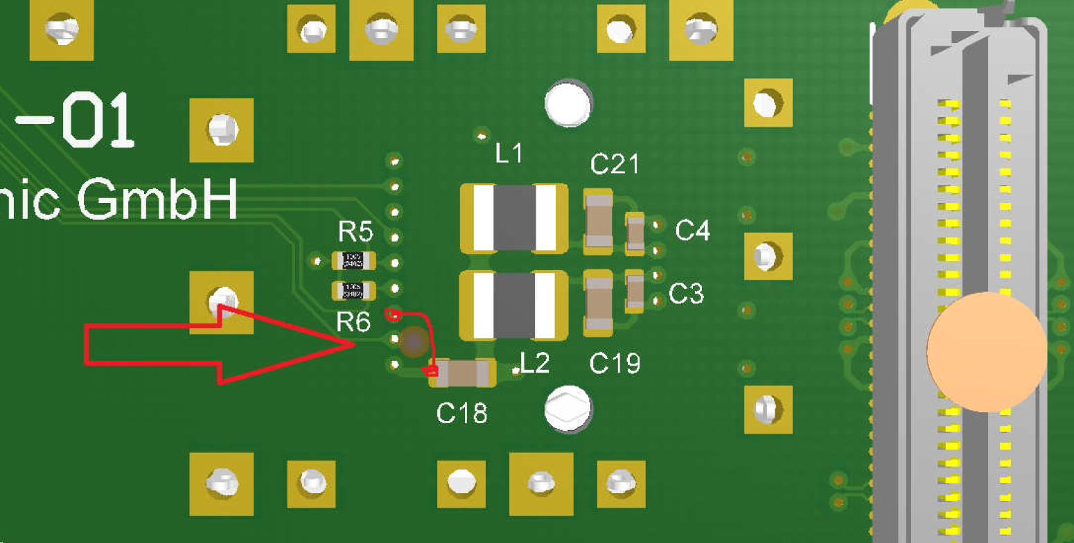
Figure 3: PCB wire patch for SFP+ connector.
...
Loop Back Circuits on B2B Connector JB1 and JB2
The TEBA0841 carrier board is mainly designed for the 4 x 5 SoMs TE0841 and TE0741. This SoMs have GTX-Transceiver units on their the FPGA -modules devices with up to 8 available MGT - lanes. To test this MGT - lanes, 5 6 RX/TX differential pairs are bridged routed in loop back circuit on-board, hence the transmitted data on this those MGT - lanes flows back to their sources its source in a loop - back circuit without intentional processing or modification.
The MGT lane pins are bridged routed on-board as fellowsfollows, if 4 x 5 SoM TE0741 TE0841 is mounted on carrier board:
| MGT Lane | B2B TX Differential Pair | B2B RX Differential Pair | B2B Pins |
|---|
| connected | |||
|---|---|---|---|
| MGT-lane 0 | JB2-8 (MGT_TX0_N) JB2-10 (MGT_TX0_P) | JB2-7 (MGT_RX0_N) JB2-9 (MGT_RX0_P) | JB2-7 to JB2-8 JB2-9 to JB2-10 |
| MGT-lane 1 | JB2-14 (MGT_TX1_N) JB2-16 (MGT_TX1_P) | JB2-13 (MGT_RX1_N) JB2-15 (MGT_RX1_P) | JB2-13 to JB2-14 JB2-15 to JB2-16 |
| MGT-lane 2 | JB2-20 (MGT_TX2_N) JB2-22 (MGT_TX2_P) | JB2-19 (MGT_RX2_N) JB2-21 (MGT_RX2_P) | JB2-19 to JB2-20 JB2-21 to JB2-22 |
| MGT-lane 7 | JB2-2 (MGT_TX7_P) JB2-4 (MGT_TX7_N) | JB2-1 (MGT_ |
RX7_ |
P) JB2- |
3 (MGT_ |
RX7_ |
N) | JB2- |
1 to JB2- |
2 JB2- |
3 to JB2- |
4 |
| MGT-lane |
| 4 | JB1-3 (MGT_ |
TX4_P) JB1-5 (MGT_ |
TX4_N) | JB1-9 (MGT_ |
RX4_P) JB1-11 (MGT_ |
RX4_N) | JB1- |
9 to JB1- |
3 JB1- |
11 to JB1- |
5 |
| MGT-lane |
| 5 | JB1-15 (MGT_ |
TX5_P) JB1-17 (MGT_ |
TX5_N) | JB1-21 (MGT_ |
RX5_P) JB1-23 (MGT_ |
RX5_N) | JB1- |
21 to JB1- |
15 JB1- |
23 to JB1- |
17 |
Table 4: Looped-backed MGT-lanes for mounted 4 x 5 SoM TE0741.TE0841
| Note |
|---|
| Note: The mounted TE 4 x 5 SoMs may have different schematic net-names of the differential signaling pairs of the MGT - lanes. See Schematic of the particular SoM. |
...
JTAG access to the mounted SoM is provided through B2B connector JB2 JB3 and is routed to the XMOD header JX1 and also to pin header J3. With the TE0790 XMOD USB2 .0 to JTAG adapter, the FPGA device of the mounted SoM can be programed via USB2 .0 interface.
JTAG Signal | B2B Connector Pin | XMOD Header JX1 | Pin Header J3 | Note |
|---|---|---|---|---|
| TCK | JB3-100 | JX1-4 | J3-4 | - |
| TDI | JB3-96 | JX1-10 | J3-10 | - |
| TDO | JB3-98 | JX1-8 | J3-8 | - |
| TMS | JB3-94 | JX1-12 | J3-12 | - |
Table 5: JTAG interface signals.
XMOD FTDI JTAG-Adapter Header JX1
The JTAG interface of the mounted SoM can be accessed via XMOD header JX1, so in use with the XMOD-FT2232H adapter-board TE0790 the mounted SoM can be programmed via USB2 .0 interface. The TE0790 board provides also an UART interface to the SoM's Zynq FPGA device which can be accessed by the USB2 .0 interface of the adapter-board while the signals between these serial interfaces will be converted.
Following table describes the signals and interfaces of the XMOD header JX1:
| Pin Schematic Name | XMOD Header JX1 Pin | B2B | Note |
|---|---|---|---|
| TCK | C (pin 4) | JB3-100 | - |
| TDO | D (pin 8) | JB3-98 | - |
| TDI | F (pin 10) | JB3-96 | - |
| TMS | H (pin 12) | JB3-94 | - |
| MIO15 | A (pin 3) | JB1-86 | UART-TX (transmit line) |
| MIO14 | B (pin 7) | JB1-91 | UART-RX (receive |
| line) |
| RESIN | G (pin 11) | JB3-17 |
| nRESET signal to the mounted SoM |
Table 6: XMOD header JX1 signals and connections.
When using XMOD FTDI JTAG Adapter TE0790, the adapter-board's VCC and VCCIO will be sourced by the on-boards 3.3V supply voltage. Set the XMOD DIP-switch with the setting:
| XMOD DIP-switches | Position |
|---|---|
| Switch 1 | ON |
| Switch 2 | OFF |
| Switch 3 | OFF |
| Switch 4 | OFF |
Table 7: XMOD adapter board DIP-switch positions for voltage configuration.
| Note |
|---|
Use Xilinx compatible TE0790 adapter board (designation TE-0790-xx with out 'L') to program the Xilinx Zynq devices. The TE0790 adapter board's CPLD have to be configured with the Standard variant of the firmware. Refer to the TE0790 Resources Site for further information and firmware download. |
...
As alternative to the XMOD header JX1, on the Carrier Board carrier board pin header J3 is present, which has a XMOD header-compatible pin-assignment, but also two additional pins (15,16) as differential pairs pair to supply the mounted SoM with an external MGT reference clock signal:
| Pin Schematic Name | Header J3 Pin | B2B | Note |
|---|---|---|---|
| TCK | 4 | JB3-100 | - |
| TDO | 8 | JB3-98 | - |
| TDI | 10 | JB3-96 | - |
| TMS | 12 | JB3-94 | - |
| MIO15 | 3 | JB1-86 | UART-TX (transmit line) |
| MIO14 | 7 | JB1-91 | UART-RX (receive line) |
| RESIN | 11 | JB3-17 | nRESET signal to the mounted SoM |
| CLK0_N | 15 | JB2-32 | AC decoupled on-board (100 nF capacitor) |
| CLK0_P | 16 | JB2-34 | AC decoupled on-board (100 nF capacitor) |
Table 8: JTAG/UART header J3 signals and connections.
UART Interface
UART interface is available on B2B connector JB1 and is usually established by MIO-pins of the PS-bank of the mounted SoM's Zynq FPGA device. With the TE0790 XMOD USB2 .0 adapter, the UART signals can be converted to USB2 .0 interface signals:
| UART Signal Schematic Name | B2B | XMOD Header JX1 | Pin Header J3 | Note |
|---|---|---|---|---|
| MIO14 | JB1-91 | JX1-7 | J3-7 | UART-RX (receive line) |
| MIO15 | JB1-86 | JX1-3 | J3-3 | UART-TX (transmit line) |
Table 9: UART interface signals.
SD IO Interface
The SD IO interface of the mounted SoM is routed to the pin header J4. Due to the different operation voltage levels of the MicroSD Card socket (3.3V) and the and the SoM's Zynq device MIO-bank (1.8V), a VDD/VCCIO translation is necessary which can be provided for example by Texas Instruments TXS02612 SDIO port expander IC. Both voltage levels are available on pin header J4:
...
Table 7: SD IO interface signals.
USB2.0 Interface
TEBA0841 board has one physical Micro USB2.0 type B socket J10, the differential data signals of the USB2.0 socket are routed to the B2B connector JB2, where they can be accessed by the corresponding USB2.0 PHY transceiver of the mounted SoM.
With Micro USB2.0 type B socket, the USB2.0 interface can also be used in Device or OTG mode.
Following table gives an overview of the USB2.0 interface signals:
...
JB2-48
...
USB2 Interface
TEBA0841 board has one physical Micro USB2 Type B socket J10, the differential data signals of the USB2 socket are routed to the B2B connector JB2, where they can be accessed by the corresponding USB2 PHY transceiver of the mounted SoM, if available.
With Micro USB2 Type B connector, the USB2 interface is usable in Device or OTG mode.
Following table gives an overview of the USB2 interface signals:
| USB2.0 Signal Schematic Name | B2B | Connected to | Note |
|---|---|---|---|
| OTG_N | JB2-48 | J10-2 | USB2 data differential pair |
| OTG_P | JB2-50 | J10-3 | |
| OTG-ID | JB2-52 | J10-4 | Ground this pin for A-Device (host), leave floating this pin for B-Device (peripheral). |
| USB-VBUS | JB2-56 | J10-1 | USB supply voltage for Host mode. Not supplied by the Carrier Board. |
Table 10: USB2 interface signals and connections
On-board Peripherals
| HTML |
|---|
<!--
Components on the Module, like Flash, PLL, PHY...
--> |
On-board LEDs
The on-board LEDs are available to the user and can be used to indicate system status and activities:
| LED | Color | Signal Schematic Name | Connected to | Description and Notes |
|---|---|---|---|---|
| D1 | Green | MIO9 | JB1-92 | available to user |
| D2 | Red | RLED | JB3-90 | available to user |
Table 11: On-board LEDs
DIP-Switch
There are one 4-bit DIP-witches S1 present on the TEBA0841 board to configure options and set parameters. The following table describes the of the particular switches:
| DIP-switch S1 | Signal Schematic Name | Connected to | Notes |
|---|---|---|---|
| S1A | BOOTMODE | JB1-90 | The functionalities of all DIP-switches is dependent on the mounted The DIP-switch sets control signals, which are usually routed to the So refer to the Wiki reference page of the SC CPLD firmware of the SoM. |
| S1B | EN1 | JB1-27 | |
| S1C | MODE | JB1-31 | |
| S1D | NOSEQ | JB1-8 |
Table 12: DIP-switch S1
Table 8: USB2.0 interface signals and connections.
On-board Peripherals
| HTML |
|---|
<!--
Components on the Module, like Flash, PLL, PHY...
--> |
On-board LEDs
The on-board LEDs are available to the user and can be used to indicate system status and activities:
...
Figure 11: On-board LEDs
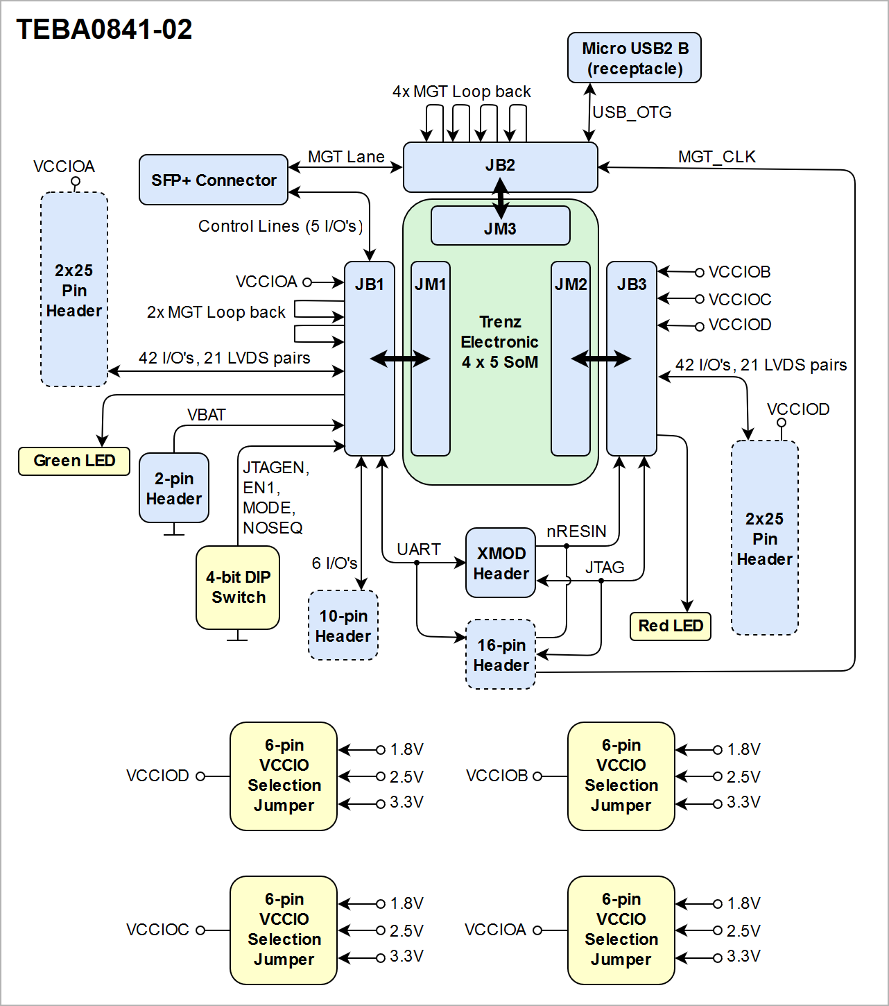
VCCIO Selection Jumper
On the TEBA0841 carrier board different VCCIO configurations can be selected by the jumper header J26, J27, J5 and J27J6.
TE 4 x 5 Modules have a standard assignment of PL-bank I/O voltages on their the B2B connectors, which will be fed with I/O voltage from base-board.
Base-board PL-bank I/O Voltages | Carrier Board B2B Pins | Standard Assignment of PL-bank I/O Voltages on TE 4x5 Modules |
|---|
| VCCIOA | JB1-10, JB1-12 | VCCIOA (JM1-9, JM1-11) |
| VCCIOB | JB3-2, JB3-4 | VCCIOB (JM1-1, JM1-3) |
| VCCIOC | JB3-6 | VCCIOC (JM1-5) |
| VCCIOD |
| JB3-8, |
| JB3-10 | VCCIOD (JM2-7, JM2-9) |
Table 1213: Base-board PL-bank I/O voltages VCCIOA and ... VCCIOD
| Note |
|---|
Note: The corresponding PL-bank I/O voltages of the 4 x 5 SoM to the selectable base-board voltages VCCIOA and ... VCCIOD are depending on the mounted 4 x 5 SoM and varying in order of the used model. Refer to the SoM's schematic for information about the specific pin assignments on module's B2B-connectors regarding the PL-bank I/O voltages and to the 4 x 5 Module integration Guide for VCCIO voltage options. |
Following table describes how to configure the base-board supply-voltages by jumpers:
Base-board PL-bank I/O Voltages | VCCIOA | VCCIOB | VCCIOC | VCCIOD |
|---|---|---|---|---|
| 1.8V | J26:1-2 | J5:1-2 | J6:1-2 | J27:1-2 |
| 2.5V | J26:3-4 | J5:3-4 | J6:3-4 | J27:3-4 |
| 3.3V |
| J26:5-6 | J5:5-6 | J6 |
| :5-6 | J27:5-6 |
Table 1314: Configuration of base-board supply-voltages via jumpers. Jumper-Notification: 'Jx: 1-2' means pins 1 and 2 are connected, 'Jx: 3-4' means pins 3 and 4 are connected, and so on.
| Note |
|---|
Take care of the VCCO voltage ranges of the particular PL IO-banks (HR, HP) of the mounted SoM, otherwise damages may occur to the FPGA. Therefore, refer to the TRM of the mounted SoM to get the specific information of the voltage ranges. It is recommended to set and measure the PL IO-bank supply-voltages before mounting of TE 4 x 5 module to avoid failures and damages to the functionality of the mounted SoM. |
...
The maximum power consumption of the Carrier Board carrier board depends mainly on the mounted SoM's FPGA design running on the Zynq device.
Xilinx provide a power estimator excel sheets to calculate power consumption. It's also possible to evaluate the power consumption of the developed design with Vivado. See also Trenz Electronic Wiki FAQ.
| Power Input | Typical Current |
|---|---|
| 3.3V | TBD* |
Table 1415: Typical power consumption.
* TBD - To Be Determined soon with reference design setup.
...
The external power-supply can be connected to the board by the following pins:
| Connector | 3.3V pin | GND pin |
|---|---|---|
| JX1 | JX1-5, JX1-6, | JX1-1, JX1-2 |
| J3 | J3-5, J3-6 | J3-1, J3-2 |
| J4 | J4-5 | J4-1, J4-2 |
| J20 | J20-5, J20-46 | J20-1 , J20-2 , J20-49 , J20-50 |
| J17 | J17-5, J17-46 | J17-1 , J17-2 , J17-49 , J17-50 |
Table 1516: Connector pins capable for external 3.3V power supply
...
The PL-bank I/O voltages 1.8V, 2.5V and 3.3V will be available after the mounted SoM's 3.3V voltage level has reached stable state on B2B-connector pins JM2-10 and JM2-12 (JB2-9, JB2-11), meaning that all on-module voltages have become stable and module is properly powered up.
Following diagram shows the distribution of the external input voltage of nominal 3.3V to the components:
| Scroll Title | ||||
|---|---|---|---|---|
|
...
|
...
|
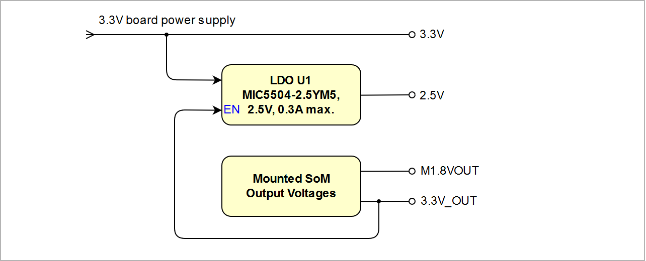
Power Rails
The voltage direction of the power rails is from board and on-board connectors' view:
| Module Connector (B2B) Designator | VCC / VCCIO | Direction | Pins | Notes |
|---|---|---|---|---|
| JB1 | 3.3V | Out | 2, 4, 6, 14, 16 | 3.3V module supply voltage |
| VCCIOA | Out | 10, 12 | PL IO-bank |
| VCCO | |||
| M1.8VOUT | In | 40 | 1.8V module output voltage |
| JB3 | 3.3V_OUT | In | 9, 11 | 3.3V module output voltage |
| 3.3V | Out | 1, 3, 5, 7 | 3.3V module supply voltage | |
| VCCIOB | Out | 2, 4 | PL IO-bank VCCO | |
| VCCIOC | Out | 6 | PL IO-bank VCCO | |
| VCCIOD | Out | 8, 10 | PL IO-bank |
| VCCO |
| JB2 | USB-VBUS | Out | 56 | USB Host supply voltage |
Table 1617: Power pin description of B2B module connector.
| On-board Pin Header Designator | VCC / VCCIO | Direction |
|---|
| Pins | Notes | |||
|---|---|---|---|---|
| J17 | 3.3V | In / Out | 5, 48 | 3.3V external supply voltage |
| VCCIOD | In / Out | 6, 45 | PL IO-bank VCCIO, depends on Jumper settings | |
| J20 |
3.3V | In / Out | 5, 48 | 3.3V external supply voltage |
| VCCIOA | In / Out | 6, 45 | PL IO-bank VCCIO, depends on Jumper settings |
| J4 | 3.3V |
| Out | 5 |
| - |
| M1.8VOUT | Out | 6 | - |
Table 18: Power Pin description of on-board connector
| Jumper / Header Designator | VCC / VCCIO | Direction | Pins | Notes |
|---|---|---|---|---|
| J26 | VCCIOA | In | 2, 4, 6 | - |
| M1.8VOUT | Out | 1 | - | |
| 2.5V | Out | 3 | - | |
| 3.3V_OUT | Out | 5 | - | |
| J27 | VCCIOD | In | 2, 4, 6 | - |
| M1.8VOUT | Out |
| 1 | - |
Table 17: Power Pin description of on-board connector.
| 2.5V | Out | 3 | - |
| 3.3V_OUT | Out | 5 | - |
| J5 | VCCIOB |
| In | 2, 4, 6 | - | |
| M1.8VOUT | Out | 1 | - |
| 2.5V | Out | 3 | - |
| Out | 5 | - |
| J6 |
| VCCIOC | In | 2, 4, 6 | - | |
| M1.8VOUT | Out | 1 | - | |
| 2.5V | Out | 3 | - | |
| 3.3V_OUT | Out | 5 | - | |
| J7 | VBAT | In | 1 | - |
Table 19Table 18: Power Pin description of VCCIO selection jumper pin header.
| Peripheral Socket Designator | VCC / VCCIO | Direction | Pins | Notes |
|---|---|---|---|---|
| J10 | USB-VBUS | In | 1 | USB Host supply voltage |
Table 1920: Power pin description of peripheral connector.
| JTAG Header Designator | VCC / VCCIO | Direction | Pins | Notes |
|---|---|---|---|---|
| JX1 (XMOD) | 3.3V | Out | 5 | connected to 3.3V external supply voltage |
| VCCJTAG | Out | 6 | ||
| J3 | 3.3V | Out | 5 | connected to 3.3V external supply voltage |
| 3.3V | Out | 6 |
Table 2021: Power pin description of XMOD/JTAG Connector.connector
Board to Board Connectors
...
Technical Specifications
Absolute Maximum Ratings
| Parameter | Min | Max | Units | Notes |
|---|---|---|---|---|
Vin supply voltage | 3.135 | 3.465 | V | 3.3V supply-voltage ± 5%, limitations of the supply voltage depend also |
Storage Temperature | -55 | 105 | °C | Molex 74441-0001 Product Specification |
Table 2122: Board absolute maximum ratings.
Recommended Operating Conditions
| Parameter | Min | Max | Units | Notes |
|---|---|---|---|---|
| Vin supply voltage | 3.135 | 3.465 | V | 3.3V supply-voltage ± 5%, limitations of the supply voltage depend also |
| Operating temperature | -40 | +85 | °C | Molex 74441-0001 Product Specification |
Table 2223: Module recommended operating conditions.
Operating Temperature Ranges
Industrial TEBA0841 carrier board operating temperature range is industrial grade: -40°C to +85°C.
The TEBA0841 Carrier Board itself is capable to be operated at industrial grade temperature range.
Please check the operating temperature range of the mounted SoM, which determine the relevant operating temperature range of the overall system.
Physical Dimensions
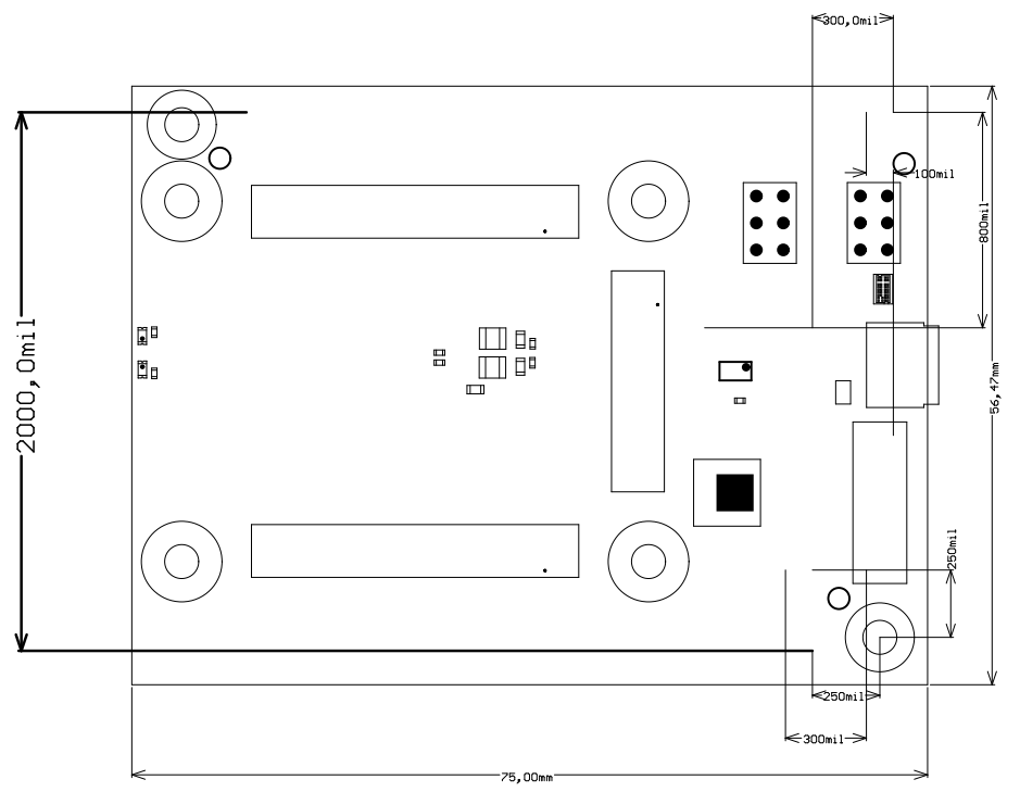
Please note that two different units are used on the figures below, SI system millimeters (mm) and imperial system .
Physical Dimensions
thousandths of an inch(mil). This is because of the 100mil pin headers used, see also explanation below. To convert mils to millimeters and vice versa use formula 100mil's = 2,54mm.
Module size: 56mm × 75mm. Board size: PCB 56.47 mm × 75 mm. Notice that some parts the are hanging slightly over the edge of the PCB like the mini USB-jacks and the SFP+ connector, which determine the total physical dimensions of the carrier board. Please download the assembly diagram for exact numbers.
Mating height of the module with standard connectors: 8mm.
PCB thickness: ca. 1.65mm.
Highest part on the PCB is the SFP+ connector, which has an approximately 11.3 mm 3mm overall hight. Please download the step model for exact numbers.
The dimensions are given in mm and mil (milli inch).
...
| Scroll Title | ||||
|---|---|---|---|---|
| ||||
|
Revision History
Hardware Revision History
| Date | Revision | Notes | PCN | Documentation Link |
|---|---|---|---|---|
| - | 02 |
| - | TEBA0841-02 |
| - | 01 |
|
| - | TEBA0841-01 |
Table 2324: Module hardware revision history.
Hardware revision number can be found on the PCB board together with the module model number separated by the dash.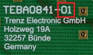
| Scroll Title | ||||
|---|---|---|---|---|
|
...
|
...
|
...
|
Document Change History
| HTML |
|---|
<!-- Generate new entry: 1.add new row below first 2.Copy "Page Information Macro(date)" Macro-Preview, Metadata Version number, Author Name and description to the empty row. Important Revision number must be the same as the Wiki document revision number 3.Update Metadata = "Page Information Macro (current-version)" Preview+1 and add Author and change description. --> |
...
Date | Revision | Contributors | Description | ||||||||||||||||||||||||||
|---|---|---|---|---|---|---|---|---|---|---|---|---|---|---|---|---|---|---|---|---|---|---|---|---|---|---|---|---|---|
|
|
|
| ||||||||||||||||||||||||||
| v.75 | Ali Naseri, Jan Kumann |
|
...
Overview
Content Tools