Page History
...
| Scroll Title | ||||||||||||||||||||||||||||||||
|---|---|---|---|---|---|---|---|---|---|---|---|---|---|---|---|---|---|---|---|---|---|---|---|---|---|---|---|---|---|---|---|---|
| ||||||||||||||||||||||||||||||||
|
...
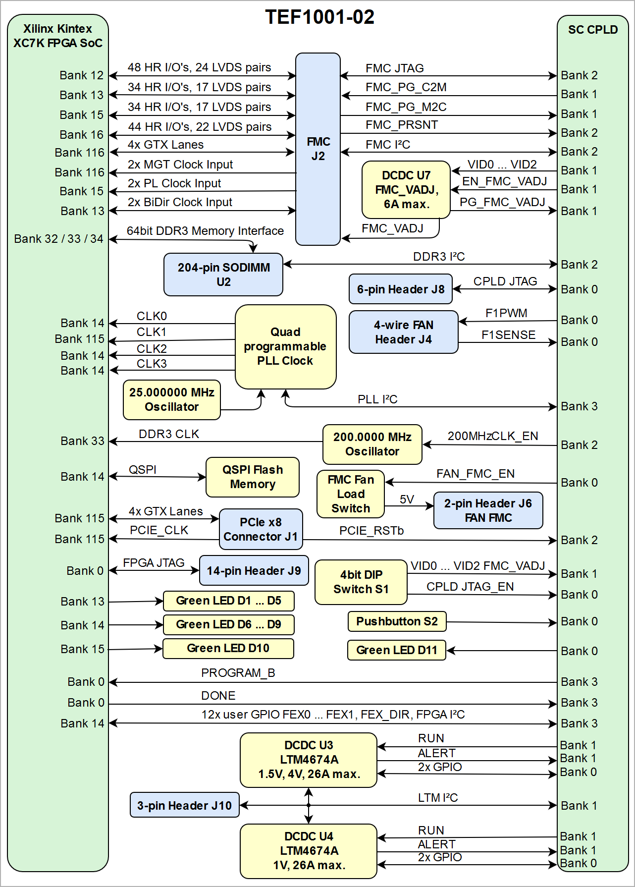
Table 6: System Controller CPLD I/O pins
| CPLD Functionality | Interface | Designated CPLD Pins | Connected to | Notes |
|---|---|---|---|---|
| I2C interface between on-board peripherals and FPGA | I2C |
|
| VCCIO: 1V8, all with pull-up to 1V8. Following devices and connectors are linked to the FPGA_IIC I2C interface:
Note: FPGA_IIC_OE must kept high for I2C operation. For I2C slave device addresses refer to the component datasheets. |
User I/Os External LVDS pairs | 10 I/Os 5 x LVDS pairs |
|
| Can also be used for single-ended signaling. |
User I/Os Internal LVDS pairs | 13 I/Os 6 x LVDS pairs |
|
| VCCIO: 1V8 Can also be used for single-ended signaling. FPGA bank 18 has also reference clock input from FMC connector (CLK2, CLK3) and clock synthesizer U9 (FCLK). Internal signal assignment: FEX_DIR <= FMC_PRSNT_M2C_L |
| FPGA programming control and state | 2 I/Os |
|
| VCCIO: 1V8 |
| I2C interface to programmable quad clock generator | I2C |
|
| VCCIO: 1V8 Only PLL_SDA has 1V8 pull-up. |
| Fan PWM control J4 | 2 I/Os |
|
| Internal signal assignment:
|
| Button S2 | 1 I/O |
|
| Functionality depends on CPLD firmware, activating pin PROGRAM_B (active low) and LED1 in standard configuration. |
| LED1 | 1 I/O |
|
| Fast blinking, when FPGA is not programmed. Internal signal assignment:
|
PCIe control line RESET_B | 1 I/O |
|
| Internal signal assignment:
|
Control interface to clock synthesizer U9 (TI LMK04828B) | SPI (3 I/Os), 4 I/Os |
|
| Pull up to 3V3PCI.
|
| Control Interface to DC-DC converters U3 and U4 (both LTM4676) | I2C (2 I/Os), 2 I/Os |
|
| 3V3 pull-ups. LTM I2C interface is also accessible trough header J10. LTM1_ALERT and LTM2_ALERT signals are not used. |
| Power-on sequence and monitoring | 6 I/Os |
|
| Sequence of the supply voltages depend on the System Controller CPLD firmware. EN_1V8, EN_3V3 and EN_FMC_VADJ will be set simultaneously at start-up. PG signals will not be evaluated. |
For detailed function of the pins and signals, the internal signal assignment and the implemented logic, look to the Wiki reference page of the module's SC CPLD or into its bitstream file.
...
| Scroll Title | ||||||||||||||||||||||||
|---|---|---|---|---|---|---|---|---|---|---|---|---|---|---|---|---|---|---|---|---|---|---|---|---|
| ||||||||||||||||||||||||
|
See also Xilinx datasheet DS892 for additional information. User should also check related base board documentation when intending base board design for TE0841 module.
...
| Scroll Title | ||||||||||||||||||||||||
|---|---|---|---|---|---|---|---|---|---|---|---|---|---|---|---|---|---|---|---|---|---|---|---|---|
| ||||||||||||||||||||||||
|
Power Rails
| Power Rail Name | B2B JM1 Pins | B2B JM2 Pins | Input/Output | Notes |
|---|---|---|---|---|
| VIN | 1, 3, 5 | 2, 4, 6, 8 | Input | Supply voltage. |
| 3.3VIN | 13, 15 | - | Input | Supply voltage. |
| B64_VCO | 9, 11 | - | Input | HR (High Range) bank voltage. |
| B66_VCO | - | 1, 3 | Input | HP (High Performance) bank voltage. |
| B67_VCO | - | 7, 9 | Input | HP (High Performance) bank voltage. |
| B68_VCO | - | 5 | Input | HP (High Performance) bank voltage. |
VBAT_IN | 79 | - | Input | RTC battery supply voltage. |
| 3.3V | - | 10, 12, 91 | Output | Module on-board 3.3V voltage level. |
Table 13: Module power rails
...
Overview
Content Tools