Page History
...
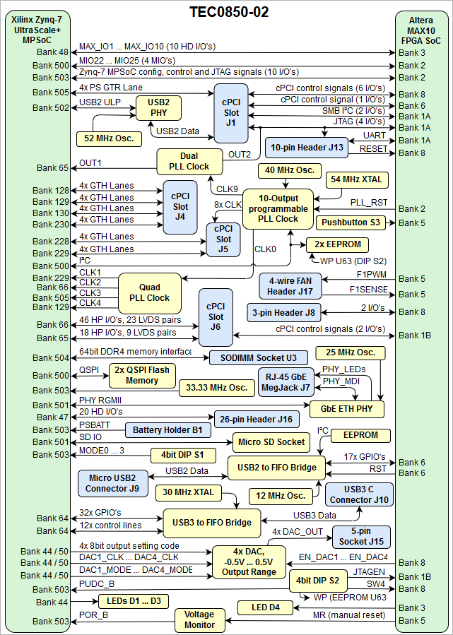
Zynq UltraScale+ MPSoC ZU15
- Front side interface connectors
- RJ-45 GbE Ethernet interface
- Elbow Socket with 4x on-board 8bit DAC output
- MicroSD Card connector
- USB2 and USB3 to FIFO bridge connector
- 4x status LEDs
- 4 CompactPCI slots for backplane connection (3U form factor)
- 24 GTH lanes
- 4 PS GTR lanes
- USB2 interface
- 64 Zynq PL HP I/O's
- 8x PLL clock input
- JTAG, I²C and 7 user I/O's to MAX10 FPGA
64bit DDR4 SODIMM (PS connected), 8 GByte maximum
Dual parallel QSPI Flash (bootable), 512 MByte maximum
- 26-pin header with 20 Zynq PL HD I/O's
- 3-pin header with 2 MAX10 FPGA I/O's
- System Controller (Altera MAX10 FPGA SoC)
- Power Sequencing
- System management and control for MPSoC and on-board peripherals
- Si5345 programmable 10 output PLL clock generator
- Si53340 Quad and Dual PLL clock generatorsgenerator
- 2x 4bit DIP switches
- 1x user push button
- Zynq MPSoC cooling FAN connector
- On-board high-efficiency DC-DC converters
...
| Scroll Title | ||||||||||||||||||||||||||||||||
|---|---|---|---|---|---|---|---|---|---|---|---|---|---|---|---|---|---|---|---|---|---|---|---|---|---|---|---|---|---|---|---|---|
| ||||||||||||||||||||||||||||||||
|
...
- GbE RJ-45 MagJack, J7
- DAC output 5-pin elbow receptacle socket, J15
- Micro USB2 B receptacle connector, J9
- MicroSD Card socket, J11
- USB C connector, J10
- LED light pipes J14 integrating LEDs D1 ... D4
- 4bit DIP-switch, S2
- 4bit DIP-switch, S1
- FTDI FT2232 USB2 to FIFO bridge, U4
- 3-pin header, J8
- MAX10 FPGA JTAG/UART 10-pin header, J13
- Altera MAX10 FPGA System Controller FPGA, U18
- 4-Wire PWM fan connector, J17
- Zynq MPSoC PL I/O 26-pin header, J16
- DDR4 SO-DIMM 260-pin socket, U3
- Battery Holder CR1220, B1
- 256 Mbit (32 MByte) Micron Serial NOR Flash Memory N25Q256A, U24
- 256 Mbit (32 MByte) Micron Serial NOR Flash Memory N25Q256A, U25
- DC-DC Converter LT8471IFE @+5VA/-5VA, U74
- DC-DC Converter EM2130L02QI @VCCINT_0V85, U17
- DC-DC Converter 171050601 @5V, U50
- Xilinx Zynq Ultrascale+ MPSoC, U1
- Si5345A 10-output I²C programmable PLL clock, U14
- Main power fuse @2.5A/16V, F1
- cPCI slot, J1
- cPCI slot, J4
- cPCI slot, J5
- cPCI slot, J6
- FTDI FT601Q USB3 to FIFO bridge, U9
- TI THS5641 8bit DAC ,U28
- TI THS5641 8bit DAC ,U31
- TI THS5641 8bit DAC ,U29
- TI THS5641 8bit DAC ,U33
- Marvell Alaska 88E1512 GbE PHY ,U20
...
| Scroll Title | ||||||||||||||||||||||||||||||||
|---|---|---|---|---|---|---|---|---|---|---|---|---|---|---|---|---|---|---|---|---|---|---|---|---|---|---|---|---|---|---|---|---|
| ||||||||||||||||||||||||||||||||
|
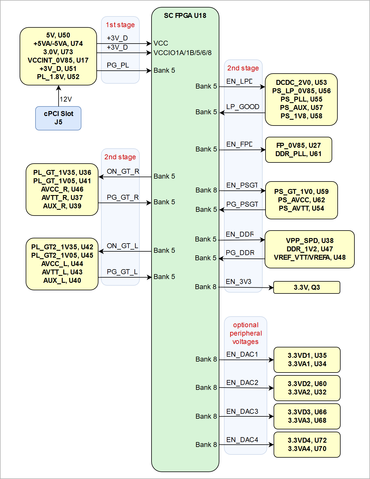
Voltage Monitor Circuit
| Scroll Title | ||||||||||||||
|---|---|---|---|---|---|---|---|---|---|---|---|---|---|---|
| ||||||||||||||
|
Power Rails
...
|
Power Rails
| Scroll Title | ||||||||||||||||||||||||||||||||||||||||||||||||||||||||||||||||||||||||||
|---|---|---|---|---|---|---|---|---|---|---|---|---|---|---|---|---|---|---|---|---|---|---|---|---|---|---|---|---|---|---|---|---|---|---|---|---|---|---|---|---|---|---|---|---|---|---|---|---|---|---|---|---|---|---|---|---|---|---|---|---|---|---|---|---|---|---|---|---|---|---|---|---|---|---|
| ||||||||||||||||||||||||||||||||||||||||||||||||||||||||||||||||||||||||||
|
Bank Voltages
| Scroll Title | |||||||||||||||||||||||||||||||||||||||||||||||||||||||||||||||||||||||||||||||||||||||||||||||||||||||||||||||||||||||||||||||||||||||||||||||
|---|---|---|---|---|---|---|---|---|---|---|---|---|---|---|---|---|---|---|---|---|---|---|---|---|---|---|---|---|---|---|---|---|---|---|---|---|---|---|---|---|---|---|---|---|---|---|---|---|---|---|---|---|---|---|---|---|---|---|---|---|---|---|---|---|---|---|---|---|---|---|---|---|---|---|---|---|---|---|---|---|---|---|---|---|---|---|---|---|---|---|---|---|---|---|---|---|---|---|---|---|---|---|---|---|---|---|---|---|---|---|---|---|---|---|---|---|---|---|---|---|---|---|---|---|---|---|---|---|---|---|---|---|---|---|---|---|---|---|---|---|---|---|---|
| |||||||||||||||||||||||||||||||||||||||||||||||||||||||||||||||||||||||||||||||||||||||||||||||||||||||||||||||||||||||||||||||||||||||||||||||
|
Technical Specifications
Absolute Maximum Ratings
...
Overview
Content Tools