...
| Scroll Title |
|---|
| anchor | Figure_1BD |
|---|
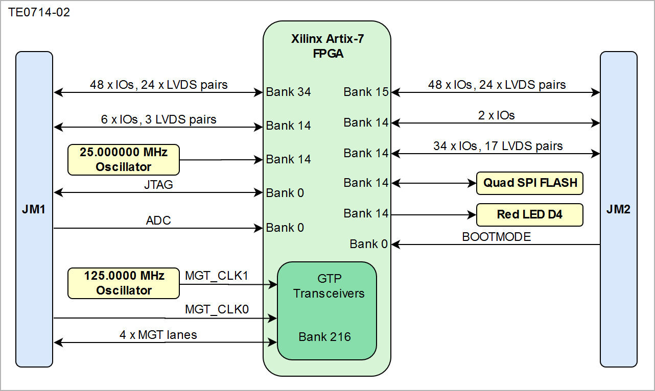
| title | Figure 1: TE0714 block diagram |
|---|
|
| Scroll Ignore |
|---|
| draw.io Diagram |
|---|
| border | truefalse |
|---|
| viewerToolbar | true |
|---|
| |
|---|
| fitWindow | false |
|---|
| diagramDisplayName | |
|---|
| lbox | true |
|---|
| revision | 4 |
|---|
| diagramName | BD-TE0714-02 |
|---|
| simpleViewer | falsetrue |
|---|
| width | |
|---|
| links | auto |
|---|
| tbstyle | top |
|---|
| diagramWidth | 641 | revision | 4 |
|---|
|
|
| Scroll Only |
|---|
|
|
Main Components
...
| Scroll Title |
|---|
| anchor | Figure_2MC |
|---|
| title | Figure 2: TE0714 main components |
|---|
|
| Scroll Ignore |
|---|
| draw.io Diagram |
|---|
| border | truefalse |
|---|
| viewerToolbar | true |
|---|
| |
|---|
| fitWindow | false |
|---|
| diagramDisplayName | |
|---|
| lbox | true |
|---|
| revision | 2 |
|---|
| diagramName | MC-TE0714 |
|---|
| simpleViewer | falsetrue |
|---|
| width | |
|---|
| links | auto |
|---|
| tbstyle | top |
|---|
| diagramWidth | 641 | revision | 2 |
|---|
|
|
| Scroll Only |
|---|
|
|
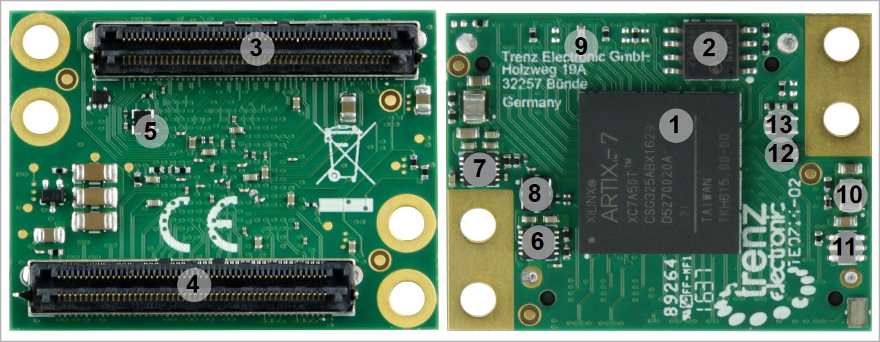
- Xilinx Artix-7 FPGA (XC7A series), U4
- 16 MByte SPI Flash, U7
- B2B connector Samtec Razor Beam™ LSHM-150, JM2
- B2B connector Samtec Razor Beam™ LSHM-150, JM1
- 25 MHz oscillator, U8
- Single output low-dropout linear regulator (1.2V_MGT), U6
- Single output low-dropout linear regulator (1.0V_MGT), U5
- Low-jitter precision LVDS 125 MHz oscillator (GT Clock), U2
- Red indication LED, D4
- Step-down DC-DC converter (1.0V), U1
- PFET load switch with configurable slew rate (3.3V), Q1
- Low-power step-down DC-DC converter (1.8V), U3
- Voltage detector for circuit initialization and timing supervision, U23
...
Initial Delivery State
| Scroll Title |
|---|
| anchor | Table_Initial_Delivery_1State |
|---|
| title | Table 1: Initial delivery state of programmable devices on the module. |
|---|
|
| Scroll Table Layout |
|---|
| orientation | portrait |
|---|
| sortDirection | ASC |
|---|
| repeatTableHeaders | default |
|---|
| style | |
|---|
| widths | |
|---|
| sortByColumn | 1 |
|---|
| sortEnabled | false |
|---|
| cellHighlighting | true |
|---|
|
Storage device name | Content | Notes |
|---|
SPI Flash OTP Area | Empty, not programmed | Except serial number programmed by flash vendor | SPI Flash Quad Enable bit | Programmed |
| SPI Flash main array | demo design |
| eFUSE USER | Not programmed |
| eFUSE Security | Not programmed |
|
|
Control Signals
| Page properties |
|---|
|
- Overview of Boot Mode, Reset, Enables,
|
Boot process is controlled by signals on the board to board (B2B) connector.
| Scroll Title |
|---|
| anchor | Table_Boot_2Signals |
|---|
| title | Table 2: Boot signals. |
|---|
|
| Scroll Table Layout |
|---|
| orientation | portrait |
|---|
| sortDirection | ASC |
|---|
| repeatTableHeaders | default |
|---|
| style | |
|---|
| widths | |
|---|
| sortByColumn | 1 |
|---|
| sortEnabled | false |
|---|
| cellHighlighting | true |
|---|
|
| Signal | Direction | Signal State | Description |
|---|
| BOOTMODE
| input | high or open | Master SPI, x4 Mode
| low or ground
| Slave SelectMAP | | PROG_B | input | pulsed low | Clear FPGA configuration (falling edge) and initiate a new configuration sequenz (next rising edge). | | DONE | output | high | Completion of configuration sequence. |
|
| Note |
|---|
SPI FPGA pins D02 and D03 have no pull-ups on the module, so with PUDC=High option, those pins are floating if there are no pull-ups on baseboard. As those pins have SPI RESET function when Quad mode is not enabled, it is mandatory to either add pull-ups on user baseboard or program the Quad Enable bit in Flash nonvolatile status register. |
...
JTAG access to the Xilinx Artix-7 FPGA device is provided through connector JM1.
| Scroll Title |
|---|
| anchor | Table_3JTAG |
|---|
| title | Table 3: JTAG signals. |
|---|
|
| Scroll Table Layout |
|---|
| orientation | portrait |
|---|
| sortDirection | ASC |
|---|
| repeatTableHeaders | default |
|---|
| style | |
|---|
| widths | |
|---|
| sortByColumn | 1 |
|---|
| sortEnabled | false |
|---|
| cellHighlighting | true |
|---|
|
Signal Name | B2B Pin |
|---|
| TCK | JM1:89 | | TDI | JM1:85 | | TDO | JM1:87 | | TMS | JM1:91 |
|
On-board LED
...
There is one LED on TE0714 module:.
| Scroll Title |
|---|
| anchor | Table_4LEDs |
|---|
| title | Table 4: LED connectionconnetion. |
|---|
|
| Scroll Table Layout |
|---|
| orientation | portrait |
|---|
| sortDirection | ASC |
|---|
| repeatTableHeaders | default |
|---|
| style | |
|---|
| widths | |
|---|
| sortByColumn | 1 |
|---|
| sortEnabled | false |
|---|
| cellHighlighting | true |
|---|
|
LED | Color | FPGA | Notes |
|---|
D4 | Red | K18 | User programmable |
|
Clock
| Scroll Title |
|---|
| anchor | Table_5Clocks |
|---|
| title | Table 5: Clock signals. |
|---|
|
| Scroll Table Layout |
|---|
| orientation | portrait |
|---|
| sortDirection | ASC |
|---|
| repeatTableHeaders | default |
|---|
| style | |
|---|
| widths | |
|---|
| sortByColumn | 1 |
|---|
| sortEnabled | false |
|---|
| cellHighlighting | true |
|---|
|
Clock | Default Frequency | IC | FPGA | Notes |
|---|
| CLK25MHz | 25 MHz | U8 | T14 | Frequency depends on the module variant. Output is compatible to 3.3V and 1.8V I/O standard of the FPGA bank. | | MGT_CLK | 125MHz | U2 | B6/B5 | Frequency depends on the module variant |
|
...
FPGA bank number and number of I/O signals connected to the B2B connector:
| Scroll Title |
|---|
| anchor | Table_6B2B |
|---|
| title | Table 6: B2B I/Os |
|---|
|
| Scroll Table Layout |
|---|
| orientation | portrait |
|---|
| sortDirection | ASC |
|---|
| repeatTableHeaders | default |
|---|
| style | |
|---|
| widths | |
|---|
| sortByColumn | 1 |
|---|
| sortEnabled | false |
|---|
| cellHighlighting | true |
|---|
|
| FPGA Bank | B2B Connector | I/O Signal Count | Voltage Level | Notes |
|---|
| 14 | JM1 | 6 | VCCIO_0 |
| | 14 | JM2 | 36 | VCCIO_0 | NB! 17 LVDS pairs possible. | | 15 | JM2 | 48 | VCCIO15 | Supplied by the baseboard. | | 34 | JM1 | 48 | VCCIO34 | Supplied by the baseboard. | | 216 | JM1 | 16 | MGT_AVCC MGT_AVTT | 4 x GTP lanes. |
|
...
| Page properties |
|---|
|
Notes : - add subsection for every component which is important for design, for example:
- Ethernet PHY
- USB PHY
- Programmable Clock Generator
- Oscillators
- eMMCs
- RTC
- FTDI
- ...
- DIP-Switches
- Buttons
- LEDs
|
...
Quad SPI Flash
On-board SPI flash memory S25FL127S (U7) is used to store initial FPGA configuration. Besides FPGA configuration, remaining free flash memory can be used for user application storage. All four SPI data lines are connected to the FPGA allowing x1, x2 or x4 data bus widths. Maximum data rate depends on the bus width and clock frequency used.
...
Power Consumption
| Scroll Title |
|---|
| anchor | Table_Power_7Consumption |
|---|
| title | Table 7: Power Consumption |
|---|
|
| Scroll Table Layout |
|---|
| orientation | portrait |
|---|
| sortDirection | ASC |
|---|
| repeatTableHeaders | default |
|---|
| style | |
|---|
| widths | |
|---|
| sortByColumn | 1 |
|---|
| sortEnabled | false |
|---|
| cellHighlighting | true |
|---|
|
| Test Condition (25 °C ambient) | VIN Current mA | Notes |
|---|
| TE0714-35, TEBT0714, empty design, GT not enabled | 110mA |
|
|
...
| Scroll Title |
|---|
| anchor | Figure_3PD |
|---|
| title | Figure 3: Power Distribution |
|---|
|
| Scroll Ignore |
|---|
| draw.io Diagram |
|---|
| border | truefalse |
|---|
| viewerToolbar | true |
|---|
| |
|---|
| fitWindow | false |
|---|
| diagramDisplayName | |
|---|
| lbox | true |
|---|
| revision | 5 |
|---|
| diagramName | PD-TE0714 |
|---|
| simpleViewer | falsetrue |
|---|
| width | |
|---|
| links | auto |
|---|
| tbstyle | top |
|---|
| diagramWidth | 641 | revision | 3 |
|---|
|
|
| Scroll Only |
|---|
|
|
Power-On Sequence
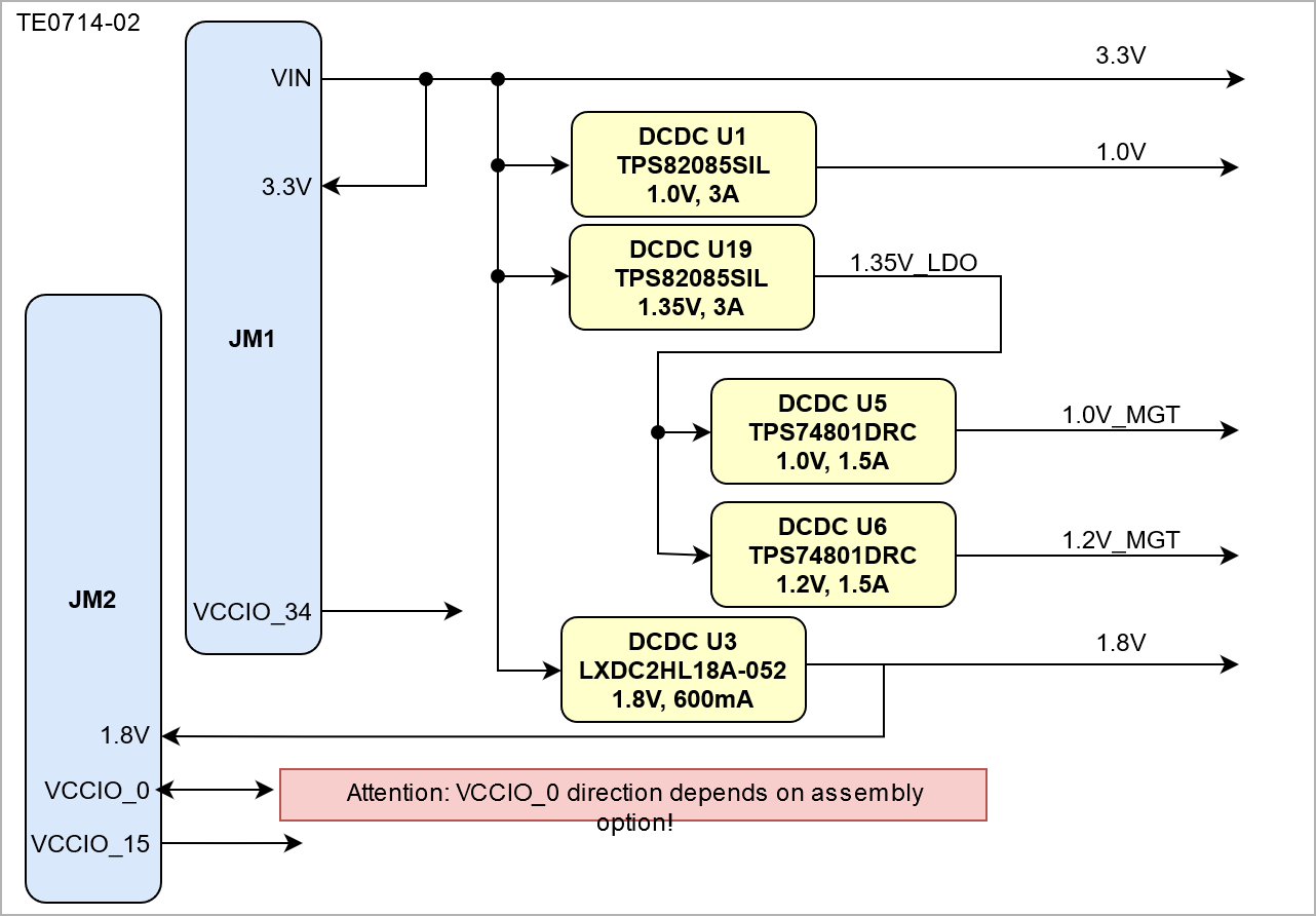
There is no specific or special power-on sequence, single power source is needed as VIN, rest of the sequence is automatic.
...
| Scroll Title |
|---|
| anchor | TableFigure_Power_8Sequency |
|---|
| title | Table 8Figure 4: Power Rails-On Sequency |
|---|
|
| tablelayout |
| orientation | portrait |
|---|
| sortDirection | ASC |
|---|
| repeatTableHeaders | default |
|---|
style | widths | | sortByColumn | 1 |
|---|
| sortEnabled | false |
|---|
| cellHighlighting | true |
|---|
| | | Direction | Note |
|---|
| VIN | 98, 100 | - | input | supply voltage |
| VCCIO_0 | - | 54 | input | high range bank voltage |
| VCCIO_15 | - | 53 | input | high range bank voltage |
| VCCIO_34 | 62 | - | input | high range bank voltage |
| 3.3V | 84 | - | output | internal 3.3V voltage level |
| 1.8V | - | 17 | output | internal 1.8V voltage level |
Bank Voltages
...
| anchor | Table_9 |
|---|
| title | Table 9: Bank Voltages |
|---|
...
...
...
...
0 Config and B14
...
1.8V or 3.3V
...
15
...
User
...
Supplied from baseboard via B2B connector, max 3.3V
...
34
...
User
...
| ignore |
|---|
| draw.io Diagram |
|---|
| border | false |
|---|
| viewerToolbar | true |
|---|
| |
|---|
| fitWindow | false |
|---|
| diagramDisplayName | |
|---|
| lbox | true |
|---|
| revision | 2 |
|---|
| diagramName | TE0714-02_Power_Sequenz |
|---|
| simpleViewer | true |
|---|
| width | |
|---|
| links | auto |
|---|
| tbstyle | top |
|---|
| diagramWidth | 641 |
|---|
|
|
| Scroll Only |
|---|
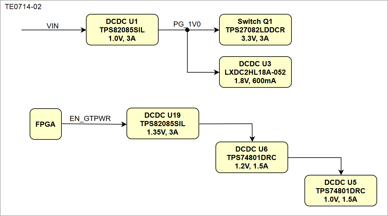 Image Added Image Added
|
|
Power Rails
| Scroll Title |
|---|
| anchor | Table__Power_Rails |
|---|
| title | Table 8: Power Rails |
|---|
|
| Scroll Table Layout |
|---|
| orientation | portrait |
|---|
| sortDirection | ASC |
|---|
| repeatTableHeaders | default |
|---|
| style | |
|---|
| widths | |
|---|
| sortByColumn | 1 |
|---|
| sortEnabled | false |
|---|
| cellHighlighting | true |
|---|
|
| | | Direction | Note |
|---|
| VIN | 98, 100 | - | input | supply voltage | | VCCIO_0 | - | 54 | input | high range bank voltage | | VCCIO_15 | - | 53 | input | high range bank voltage | | VCCIO_34 | 62 | - | input | high range bank voltage | | 3.3V | 84 | - | output | internal 3.3V voltage level | | 1.8V | - | 17 | output | internal 1.8V voltage level |
|
Bank Voltages
| Scroll Title |
|---|
| anchor | Table_Bank_Voltages |
|---|
| title | Table 9: Bank Voltages |
|---|
|
| Scroll Table Layout |
|---|
| orientation | portrait |
|---|
| sortDirection | ASC |
|---|
| repeatTableHeaders | default |
|---|
| style | |
|---|
| widths | |
|---|
| sortByColumn | 1 |
|---|
| sortEnabled | false |
|---|
| cellHighlighting | true |
|---|
|
| | |
|---|
0 Config and B14 | 1.8V or 3.3V | Depends on module variant | 15 | User | Supplied from baseboard via B2B connector, max 3.3V | 34 | User | Supplied from baseboard via B2B connector, max 3.3V |
|
Board to Board Connectors
Board to Board Connectors
| Page properties |
|---|
|
- This section is optional and only for modules.
- use "include page" macro and link to the general B2B connector page of the module series, for example: 4 x 5 SoM LSHM B2B Connectors
|
...
Absolute Maximum Ratings
| Scroll Title |
|---|
| anchor | Table_Absolute_Maximum_10Ratings |
|---|
| title | Table 10: Module absolute maximum ratings. |
|---|
|
| Scroll Table Layout |
|---|
| orientation | portrait |
|---|
| sortDirection | ASC |
|---|
| repeatTableHeaders | default |
|---|
| style | |
|---|
| widths | |
|---|
| sortByColumn | 1 |
|---|
| sortEnabled | false |
|---|
| cellHighlighting | true |
|---|
|
| Parameter | Min | Max | Units | Reference Document |
|---|
VIN supply voltage | -0.1 | 6.0 | V | - | | HR I/O banks supply voltage (VCCO) | -0.5 | 3.6 | V | Xilinx datasheet DS181 | | HR I/O banks input voltage | -0.4 | VCCO + 0.55 | V | Xilinx datasheet DS181 | | GTP transceivers Tx/Rx input voltage | -0.5 | 1.26 | V | Xilinx datasheet DS181 | Voltage on module JTAG pins | -0.4 | VCCO_0 + 0.55 | V | Xilinx datasheet DS181 | Storage temperature | -40 | +85 | °C | - |
|
Recommended Operating Conditions
| Scroll Title |
|---|
| anchor | Table_Recommended_Operating_11Conditions |
|---|
| title | Table 11: Recommended Operating Conditions |
|---|
|
| Scroll Table Layout |
|---|
| orientation | portrait |
|---|
| sortDirection | ASC |
|---|
| repeatTableHeaders | default |
|---|
| style | |
|---|
| widths | |
|---|
| sortByColumn | 1 |
|---|
| sortEnabled | false |
|---|
| cellHighlighting | true |
|---|
|
| Parameter | Min | Max | Units | Reference Document |
|---|
| VIN supply voltage | 3.135 | 3.45 | V | - | | HR I/O banks supply voltage (VCCO) | 1.14 | 3.465 | V | Xilinx datasheet DS181 | | HR I/O banks input voltage | -0.20 | VCCO + 0.20 | V | Xilinx datasheet DS181 | | Voltage on module JTAG pins | 3.135 | 3.465 | V | Xilinx datasheet DS181 |
|
...
All dimensions are shown in mm. Additional sketches, drawings and schematics can be found here.
| Scroll Title |
|---|
| anchor | Figure_4 |
|---|
| title | Figure 4: Physical dimensions drawing |
|---|
|
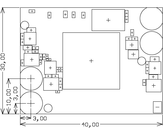 Image Removed Image Removed Image Removed Image Removed
|
Weight
found here.
| Scroll Title |
|---|
| anchor | TableFigure_Physical_12Dimensions |
|---|
| title | Table 12: Module Wight | Figure 4: Physical dimensions drawing |
|---|
|
| Image Added Image Added | Scroll Table Layout |
|---|
|
| orientation | portrait |
|---|
| sortDirection | ASC |
|---|
| repeatTableHeaders | default |
|---|
style | widths | | sortByColumn | 1 |
|---|
| sortEnabled | false |
|---|
| cellHighlighting | true |
|---|
| Variant | Weight in g | Note |
|---|
2IC6 | 8.3 | Plain Module
Variants Currently In Production
| Scroll Title |
|---|
| anchor | Table_13TE_Shop_Overview |
|---|
| title | Table 1312: Trenz Electronic Shop Overview |
|---|
|
| Scroll Table Layout |
|---|
| orientation | portrait |
|---|
| sortDirection | ASC |
|---|
| repeatTableHeaders | default |
|---|
| style | |
|---|
| widths | |
|---|
| sortByColumn | 1 |
|---|
| sortEnabled | false |
|---|
| cellHighlighting | true |
|---|
|
|
...
Hardware Revision History
| Scroll Title |
|---|
| anchor | Table_14 |
|---|
| title | Table 14: Module absolute maximum ratings. |
|---|
| | Scroll Table Layout |
|---|
| orientation | portrait |
|---|
| sortDirection | ASC |
|---|
| repeatTableHeaders | default |
|---|
style | widths | | sortByColumn | 1 |
|---|
| sortEnabled | false |
|---|
| cellHighlighting | true |
|---|
| Date | Revision | Note | PCN | Documentation Link |
|---|
| 2018-11-01 | 02 | Replace obsolete SPI Flash | in preparation | TE0714-02 |
| 2016-08-04 | 02 | VCCIO0 added to B2B | PCN-20160815 | TE0714-02 |
01 | - | - | TE0714-01 |
Hardware revision number is printed on the PCB board next to the module model number separated by the dash.
 Image Removed
...
| _Hardware_Revision_History | | title | Table 13: Hardware Revision History |
|---|
|
| Scroll Table Layout |
|---|
| orientation | portrait |
|---|
| sortDirection | ASC |
|---|
| repeatTableHeaders | default |
|---|
| style | |
|---|
| widths | |
|---|
| sortByColumn | 1 |
|---|
| sortEnabled | false |
|---|
| cellHighlighting | true |
|---|
|
|
Hardware revision number is printed on the PCB board next to the module model number separated by the dash.
Image Added
Document Change History
| Scroll Title |
|---|
| anchor | Table_Document_Change_History |
|---|
| title | Table 14: Document change history |
|---|
|
| Scroll Table Layout |
|---|
| orientation | portrait |
|---|
| sortDirection | ASC |
|---|
| repeatTableHeaders | default |
|---|
| style | |
|---|
| widths | |
|---|
| sortByColumn | 1 |
|---|
| sortEnabled | false |
|---|
| cellHighlighting | true |
|---|
|
Date | Revision | Authors | Description |
|---|
| Page info |
|---|
| modified-date |
|---|
| modified-date |
|---|
| dateFormat | yyyy-MM-dd |
|---|
|
| | Page info |
|---|
| infoType | Current version |
|---|
| prefix | v. |
|---|
| type | Flat |
|---|
| showVersions | false |
|---|
|
| |
|
...
| | type | Flat |
|---|
| showVersions | false |
|---|
|
| - Updated to TRM version 2.1
| | 2018-09-17 | V.38 | Martin Rohrmüller |
|
...
| - Added power rail section
- Added Rev 02 Flash PCN
- corrected table headings
| | 2018-09-17 | v.36 | Martin Rohrmüller | | | 2018-04-04 | | Martin Rohrmüller | Corrected clock net designator in table. | | 2017-05-28 | | Jan Kumann | Board-to-Board I/O section added. New physical dimensions images. Documents sections rearranged. | | 2017-03-20 | | John Hartfiel | Notes on Clocking section. | | 2017-01-27 | v.25 | Jan Kumann | New block diagram. | | 2016-12-01 | | Jan Kumann | Changes in the document structure, few corrections. | | 2016-11-18 | v.14
| Thorsten Trenz, Emmanuel Vassilakis | Hardware revision 02 specific changes. | 2016-06-01 | | | Initial version. |
|
Disclaimer
...
| Include Page |
|---|
| IN:Legal Notices |
|---|
| IN:Legal Notices |
|---|
|
Refer to https://wiki.trenz-electronic.de/display/PD/TE0713+TRM for online version of this manual and the rest of available documentation.