...
| Scroll Title |
|---|
| anchor | Figure_OV_BD |
|---|
| title | TE0701-06 block diagram |
|---|
|
| Scroll Ignore |
|---|
true| false | | viewerToolbar | true |
|---|
| |
|---|
| fitWindow | false |
|---|
| diagramName |
|---|
|
TE0706-01 | TE0701 block diagram | | simpleViewer | false |
|---|
| width | |
|---|
| links | auto |
|---|
| tbstyle | hidden |
|---|
| diagramDisplayName | |
|---|
| lbox | true |
|---|
| diagramWidth | 641 |
|---|
|
| | revision | 1 |
|---|
| Scroll Only |
|---|
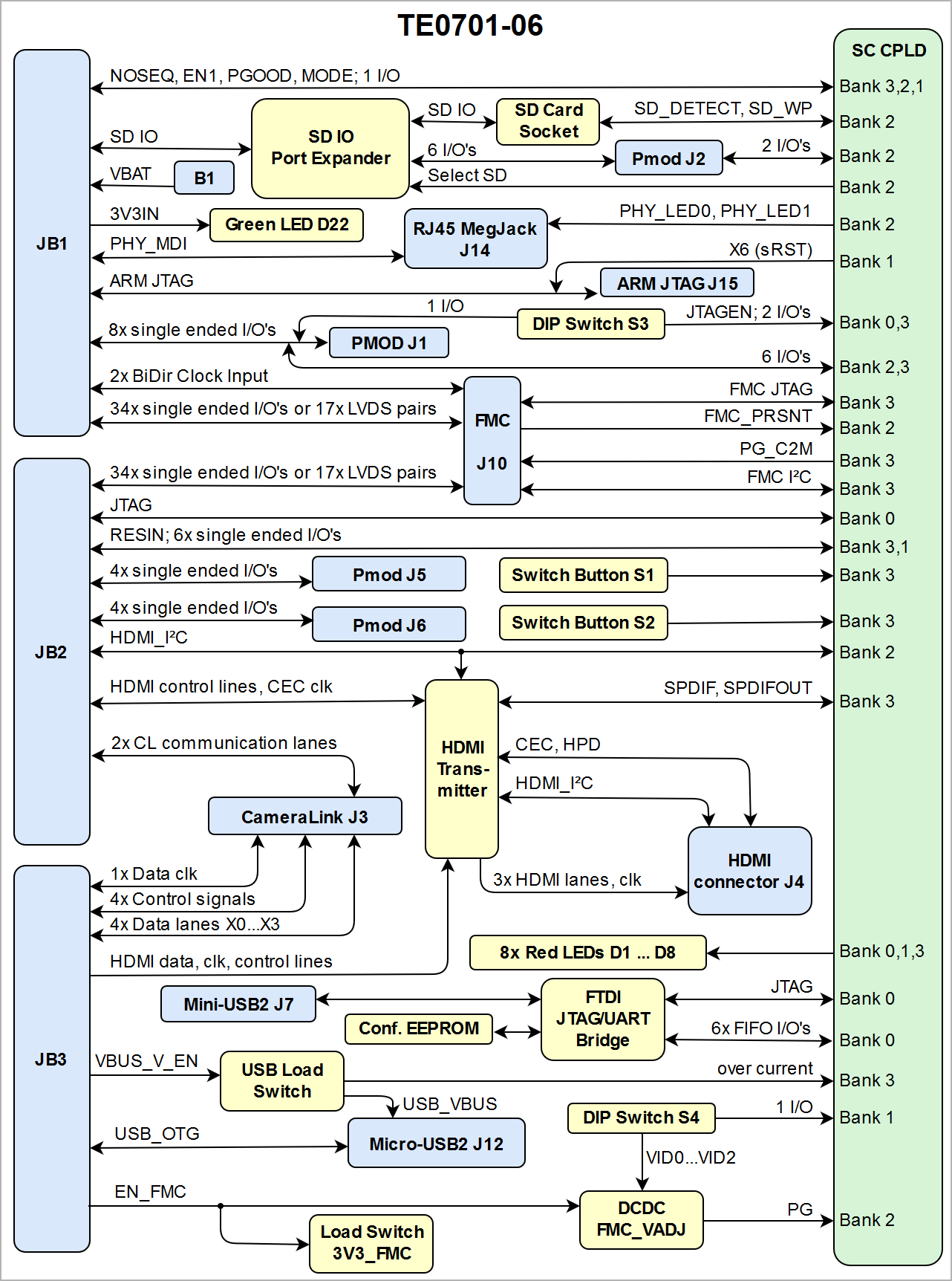 Image Added Image Added
|
|
Main Components
| Page properties |
|---|
|
Notes : - Picture of the PCB (top and bottom side) with labels of important components
- Add List below
|
| Scroll Title |
|---|
| anchor | Figure_OV_MC |
|---|
| title | TE0701-06 main components |
|---|
|
| Scroll Ignore |
|---|
| draw.io Diagram |
|---|
| border | truefalse |
|---|
| viewerToolbar | true |
|---|
| |
|---|
| fitWindow | false |
|---|
| diagramDisplayName | |
|---|
| lbox | true |
|---|
| revision | 1 |
|---|
| diagramName | TE0701 main components |
|---|
| simpleViewer | false |
|---|
| width | |
|---|
| links | auto |
|---|
| tbstyle | hidden |
|---|
| diagramWidth | 641 | revision | 1 |
|---|
|
|
| Scroll Only |
|---|
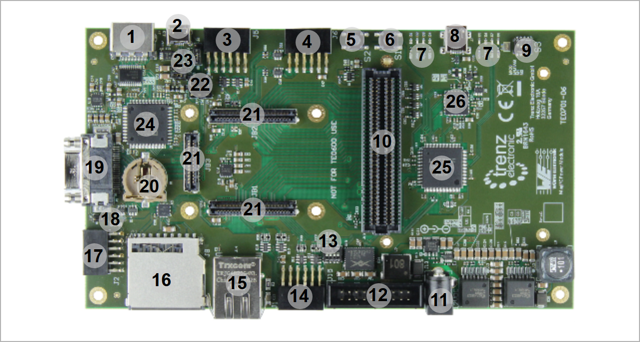 Image Added Image Added
|
|
- HDMI connector (1.4 HEAC support), J4
- Micro-USB2 connector, J12
Pmod connector, J5
- Pmod connector, J6
- User push-button ("RESTART" button by default), S2
- User push-button ("RESET" button by default), S1
- 8x red user LEDs, D1 ... D8
- Mini-USB2 connector, J7
- User 4-bit DIP switch, S3
- VITA 57.1 compliant LPC FMC connector, J10
- Barrel jack for 12V power supply, J13
- ARM JTAG connector (DS-5 D-Stream), J15
- User 4-bit DIP switch, S4
- Pmod connector, J1
- RJ45 Gigabit Ethernet connector, J14
- SD Card connector, J8
- Pmod connector, J2
- Jumper, J18
- Mini CameraLink connector, J3
- CR1220 Backup-Battery holder, B1
- Trenz Electronic 4 x 5 modules B2B connectors, JB1 ... JB3
- Jumper J16, J17, J21
- Jumper J9, J19, J20
- Analog Devices ADV7511 HDMI Transmitter, U1
- Lattice Semiconductor MachXO2 1200 HC System Controller CPLD, U14
- FTDI FT2232H USB2 to JTAG/UART Bridge, U3
...
| Scroll Title |
|---|
| anchor | Figure_SIP_JTAG/UART |
|---|
| title | JTAG/UART interface |
|---|
|
| Scroll Ignore |
|---|
| draw.io Diagram |
|---|
| border | truefalse |
|---|
| viewerToolbar | true |
|---|
| |
|---|
| fitWindow | false |
|---|
| diagramDisplayName | |
|---|
| lbox | true |
|---|
| revision | 1 |
|---|
| diagramName | TE0701 MiniUSB2 interface |
|---|
| simpleViewer | false |
|---|
| width | |
|---|
| links | auto |
|---|
| tbstyle | hidden |
|---|
| diagramWidth | 641 |
|---|
| revision | 1 |
|---|
|
|
| Scroll Only |
|---|
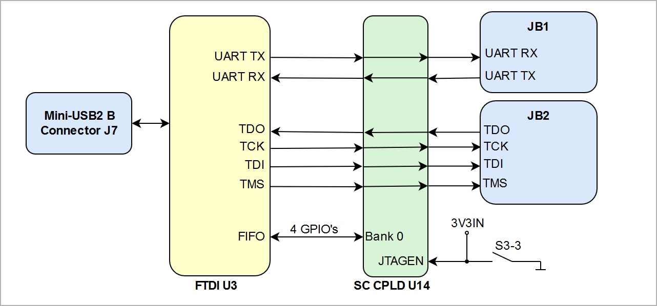 Image Added Image Added
|
|
Micro-USB2 Connector
The TE0701 carrier board can be configured as a USB host. Hence, it must provide from 5.25V to 4.75V to the board side of the downstream connection (micro-USB port on J12). To provide sufficient power, a TPS2051 power distribution switch is located on the carrier board in between the 5V power supply and the VBUS signal of the USB downstream port interface. If the output load exceeds the current-limit threshold, the TPS2051 limits the output current and pulls the over-current logic output (OC_n) low, which is routed to the on-board CPLD. The TPS2051 is put into operation by setting J19 CLOSED. J20 provides an extra 200µF decoupling capacitor (in addition to 10µF) to further stabilize the output signal. Moreover, a series terminating resistor of either 1K (J9: 1-2, 3) or 10K (J9: 1, 2-3) is selectable on the "USB-VBUS" signal. Both signals, USB-VBUS and VBUS_V_EN (that enables the TPS2051 on "high") are routed (as well as the corresponding D+/- data lines) via the on-board connector directly to the USB 2.0 high-speed transceiver PHY of the mounted SoM. In summary, the default jumper settings are the following: J9: 1-2, 3 (1K series terminating resistor); J19: CLOSED (TPS2051 in operation); J20: CLOSED (200 µF added).
| Scroll Title |
|---|
| anchor | Figure_SIP_MicroUSB2 |
|---|
| title | TE0701 MicroUSB2 interface configuration |
|---|
|
| Scroll Ignore |
|---|
| draw.io Diagram |
|---|
| border | truefalse |
|---|
| viewerToolbar | true |
|---|
| |
|---|
| fitWindow | false |
|---|
| diagramDisplayName | |
|---|
| lbox | true |
|---|
| revision | 1 |
|---|
| diagramName | TE0701 MicroUSB2 interface |
|---|
| simpleViewer | false |
|---|
| width | |
|---|
| links | auto |
|---|
| tbstyle | hidden |
|---|
| diagramWidth | 641 |
|---|
| revision | 1 |
|---|
|
|
| Scroll Only |
|---|
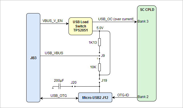 Image Added Image Added
|
|
MMC/SD-Card Socket
MMC/SD-Card socket is not directly wired to the B2B connector pins, but through a Texas Instruments TXS02612 SDIO Port Expander, which is needed for voltage translation due to different voltage levels of the Micro SD Card and MIO-bank of the Xilinx Zynq module. The Micro SD Card has 3.3V signal voltage level, but the MIO-bank on the Xilinx Zynq module has VCCIO of 1.8V.
...
| Scroll Title |
|---|
| anchor | Figure_PWR_PD |
|---|
| title | Power Distribution |
|---|
|
| Scroll Ignore |
|---|
| draw.io Diagram |
|---|
| border | truefalse |
|---|
| viewerToolbar | true |
|---|
| |
|---|
| fitWindow | false |
|---|
| diagramDisplayName | |
|---|
| lbox | true |
|---|
| revision | 1 |
|---|
| diagramName | TE0701 power distribution diagram |
|---|
| simpleViewer | false |
|---|
| width | |
|---|
| links | auto |
|---|
| tbstyle | hidden |
|---|
| diagramWidth | 641 | revision | 1 |
|---|
|
|
| Scroll Only |
|---|
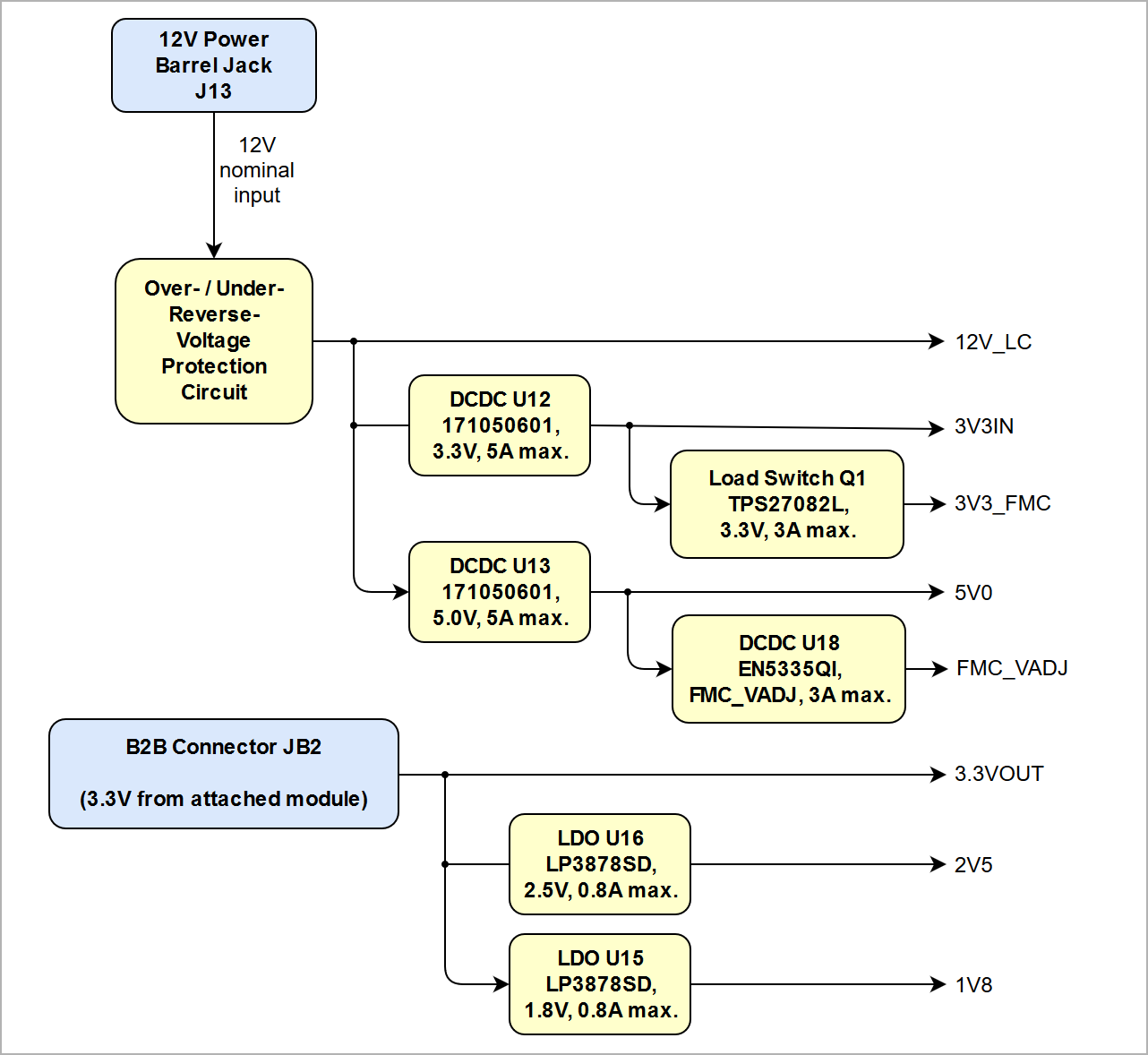 Image Added Image Added
|
|
Power-On Sequence
The on-board voltages 3.3V and 5.0V of the carrier board will be powered up simultaneously when 12V power supply is connected to the barrel jack J10.
...
| Scroll Title |
|---|
| anchor | Figure_PWR_PS |
|---|
| title | Power Sequency |
|---|
|
| Scroll Ignore |
|---|
| draw.io Diagram |
|---|
| border | truefalse |
|---|
| viewerToolbar | true |
|---|
| |
|---|
| fitWindow | false |
|---|
| diagramDisplayName | |
|---|
| lbox | true |
|---|
| revision | 1 |
|---|
| diagramName | TE0701 power-on sequence diagram |
|---|
| simpleViewer | false |
|---|
| width | |
|---|
| links | auto |
|---|
| tbstyle | hidden |
|---|
| diagramWidth | 641 |
|---|
| revision | 1 |
|---|
|
|
| Scroll Only |
|---|
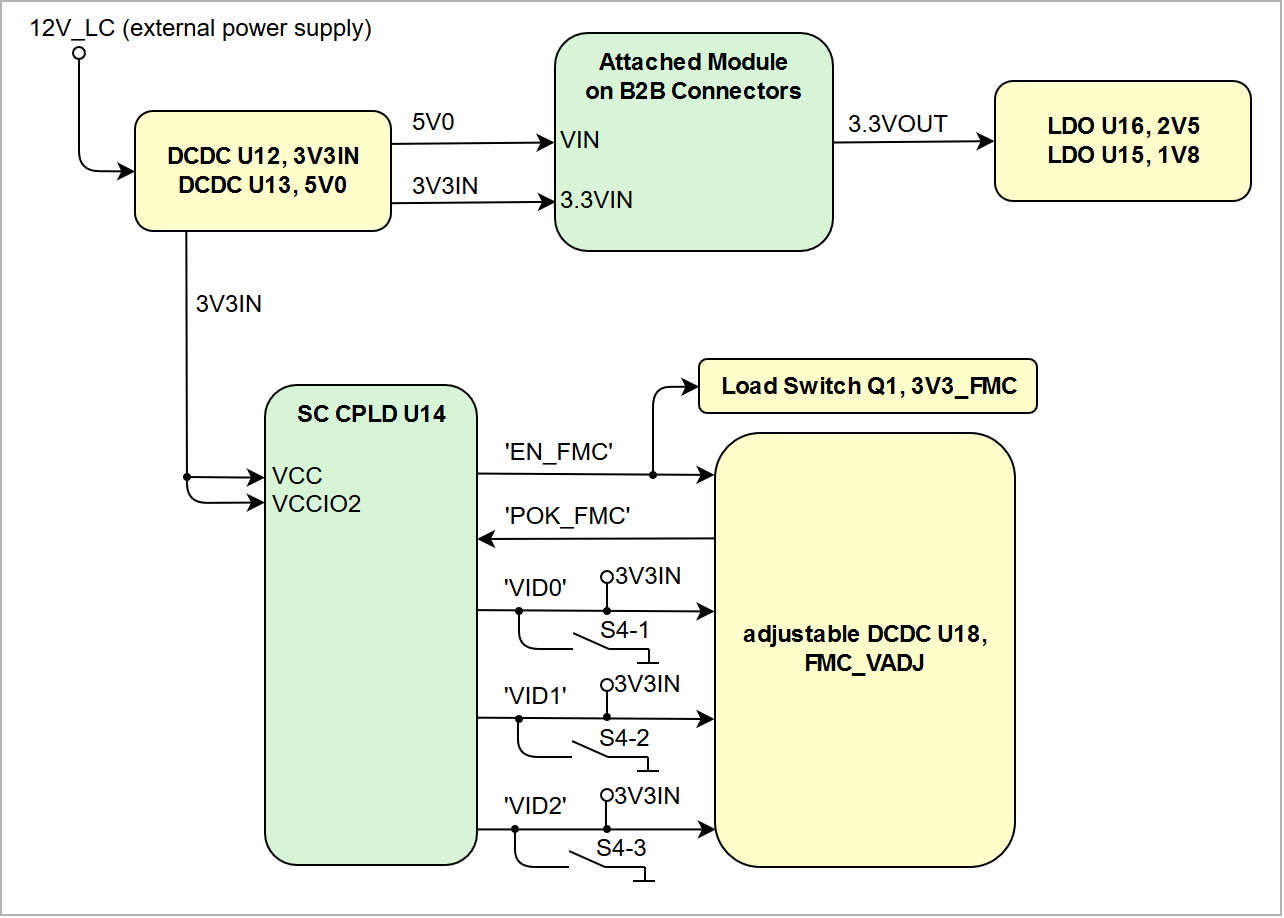 Image Added Image Added
|
|
Configuring mounted SoM's PL bank VCCO FMC_VADJ
...
There are two baseboard supply voltages VIOTA and VIOTB connected to the 4 x 5 SoM's PL IO-bank. The supply-voltages have following pin assignments on B2B-connectors:
...