Page History
...
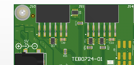
The Trenz Electronic TEB0724-01 02 is a developement carrier board for the TE0724 and compatible modules. It facilitates easy access to all on the module available features.
...
| Scroll Title | ||||||||||||||||||||||||||||||||
|---|---|---|---|---|---|---|---|---|---|---|---|---|---|---|---|---|---|---|---|---|---|---|---|---|---|---|---|---|---|---|---|---|
| ||||||||||||||||||||||||||||||||
|

...
| Scroll Title | ||||||||||||||||||||||||||||||||||||||||||||||||||||||||||||
|---|---|---|---|---|---|---|---|---|---|---|---|---|---|---|---|---|---|---|---|---|---|---|---|---|---|---|---|---|---|---|---|---|---|---|---|---|---|---|---|---|---|---|---|---|---|---|---|---|---|---|---|---|---|---|---|---|---|---|---|---|
| ||||||||||||||||||||||||||||||||||||||||||||||||||||||||||||
|


Table 1: TE0724-01 02 main components.
- Module connector for 4,0x6.0 cm module
- Pmods usabel as dual Pmods, J10, J11, J12, J13, J14, J15, J16, J17
- Pmod (single), J20
- I2C Pmod, J21
- CAN screw terminal, J2
- 5V 2.1mm input jack, J18
- microUSB J4
- USB to JTAG/UART bridge FT2232H, U1
- Configuration EEPROM U3
- RJ45 Gigabit Ehternet Jack, J3
- Power Button, S1
- Reset Button, S3
- User Button PS, S5
- User LED (green) PS, D8
- 2x User Button PL, S2, S4
- 6x User LEDs (red) PL, D2-D7
- Power LED (green), D36
- 2x10 Pin header for Boot and Programming options, J6
- 2x6 Pin header for jumper setting of CAN bus termination resistors, J22
- microSD Card Slot, J5
- Dip switches for selecting B_VCCIO_35, S6
- DCDC (B_VCCIO_35), U8
- DCDC (B_3.3V), U7
Initial Delivery State
Not programmed.
...
Table 13: On-board Push Buttons.
Pin Header
Pin Header J6 provides access to power functions, bootmode selection and PMIC In-Circuit Programming.
Dip-Switches
Dip-switch S6-1..3 are used to select the adjustable board power. Tabel 14 shows the signals, table 15 how to adjust the switches for corresponding B_VCCIO_35 Voltages.
| Switch | Signal |
|---|---|
| S6-1 | VADJ_VS0 |
| S6-2 | VADJ_VS1 |
S6-3 | VADJ_VS2 |
| S6-4 | NC |
Table 14: Dip-Switches.
| B_VCCIO_35 | S6-1 | S6-2 | S6-3 |
|---|---|---|---|
| 3.3V | OFF | OFF | OFF |
| 2.5V | OFF | OFF | ON |
1.8V | OFF | ON | OFF |
| 1.5V | OFF | ON | ON |
| 1.25V | ON | OFF | OFF |
| 1.2V | ON | OFF | ON |
Table 15: Select B_VCCIO_35 via Dip-Switches.
Pin Header
Pin Header J6 provides access to power functions, bootmode selection and PMIC In-Circuit Programming.
| PIN | PIN | Signal | B2B |
|---|---|---|---|
| J6-1 | VIN | J1-154, J1-156, J1-158, J1-160 | |
| J6-2 | VIN | J1-154, J1-156, J1-158, J1-160 | |
| J6-3 | GND | ||
| J6-4 | GND | ||
| J6-5 | I2C_SCL | J1-142 | |
| J6-6 | VBAT | J1-152 | |
| J6-7 | I2C_SDA | J1-144 | |
| J6-8 | PWR_GPIO2 | J1-143 | |
| J6-9 | ONKEY | J1-148 | |
| J6-10 | PWR_GPIO4 | J1-141 | |
| J6-11 | PWR_TP | J1-146 | |
| J6-12 | RESETREQ | J1-150 | |
| J6-13 | MODE0 | J1-2 | |
| J6-14 | GND | ||
| J6-15 | MODE1 | J1-4 | |
| J6-16 | GND |
Table 14: Pin Header J6.16: Pin Header J6.
Alternatively to selecting B_VCCIO_35 by using S6 dip switches, VCCIO_35 ( e.g. SoM TE0724, Bank 35) can be selected by removing R45 and adding a jumper on optional J19. In table 16 18 valid Jumper jumper positions are given. Voltages and maximum current ratings could be found in the corresponding TRM of the attached module, (e.g. TE0724 TRM#PowerRails ).
| PIN | Signal | B2B |
|---|---|---|
| J19-1 | VLDO1 | J1-83 |
| J19-2 | GND | |
| J19-3 | VCCIO_35 | J1-54 |
| J19-4 | VLDO2 | J1-94 |
J19-5 | VLDO34 | J1-53 |
| J19-6 | GND |
Table 1517: Optional Pin Header J19.
| Jumper position | Signal | e.g. TE0724 | |||||||||||||||||||||||||||||
|---|---|---|---|---|---|---|---|---|---|---|---|---|---|---|---|---|---|---|---|---|---|---|---|---|---|---|---|---|---|---|---|
| J19 1-3 | VLDO1 | 3.3V | ||||||||||||||||||||||||||||
| J19 4-3 | VLDO2 | 1,8V | ||||||||||||||||||||||||||||
| J19 5-3 | VLDO34 | 2,5V |
Table 1618: J19 Jumper settings for VCCIO_35 voltage selection.
...
| PIN | Signal | B2B |
|---|---|---|
| J8-1 | 3.3V | J1-43, J1-74 |
| J8-2 | GND | |
| J8-3 | S4 | J1-126 |
| J8-4 | S2 | J1-124 |
| J8-5 | ULED5 | J1-130 |
| J8-6 | ULED6 | J1-128 |
| J8-7 | ULED3 | J1-134 |
| J8-8 | ULED4 | J1-132 |
| J8-9 | ULED1 | J1-138 |
| J8-10 | ULED2 | J1-136 |
Table 1719: Optional Pin Header J8.
Optional pin header J7 gives access to otherwise not used PS MIO IOs at a 3.3V bank.
| PIN | Signal | B2B |
|---|---|---|
| J7-1 | 3.3V | 43, 74 |
| J7-2 | GND | |
| J7-3 | GND | |
| J7-4 | MIO8 | J1-14 |
| J7-5 | MIO10 | J1-31 |
| J7-6 | MIO11 | J1-33 |
| J7-7 | MIO12 | J1-35 |
| J7-8 | MIO13 | J1-37 |
| J7-9 | MIO14 | J1-39 |
| J7-10 | MIO15 | J1-41 |
Table 1820: Optional Pin Header J7.
Optional pin header J9 gives access to otherwise not used PS MIO IOs at a 1.8V bank.
| PIN | Signal | B2B |
|---|---|---|
| J9-1 | 1.8V | J1-63 |
| J9-2 | GND | |
| J9-3 | GND | |
| J9-4 | MIO_46 | J1-32 |
| J9-5 | MIO_50 | J1-40 |
| J9-6 | MIO_PB | J1-42 |
Table 1921: Optional Pin Header J9.
Power and Power-On Sequence
...
| Power Input | Typical Current |
|---|---|
| VIN | 340 mA |
Table 2022: Typical power consumption.
...
| Scroll Title | ||||||||||||||||||||||||||||||||
|---|---|---|---|---|---|---|---|---|---|---|---|---|---|---|---|---|---|---|---|---|---|---|---|---|---|---|---|---|---|---|---|---|
| ||||||||||||||||||||||||||||||||
|

User should also check related module documentation and Xilinx data sheet, respectively.
...
The power-on sequence is solely controlled by the attached module. The baseboard DCDC regulators U7 and U8 are enabled by the 3.3V rail of the module. Optional sequenzing signals for integration of additional hardware are PWR_GPIO2 and PWR_GPIO4. If the attached module uses the adjustable bank power VCCIO_35, this has to be powered up after the modules SOCs powerrails are up and before any other signal is applied to the bank IOs. The 1.8V and 3.3V power rails are used for the SD Card level shifter U13. The datasheet states to first power up 1.8V and then 3.3V, this has to be taken into account when reconfiguring the power circuit of the attached SoM.
...
Power Rail Name | B2B J1 Pins | Direction on B2B | Notes | ||
|---|---|---|---|---|---|
| VIN | 154, 156, 158, 160 | Output | 160 | Output | External main supply voltage (5V). |
| B_3.3V | - | - | Onboard DCDC. | ||
| B_VCCIO_35 | - | - | Onboard adjustable DCDCExternal main supply voltage (5V). | ||
| 3.3V | 43, 74 | Input | |||
1.8V | 63 | Input | |||
| VCCIO_35 | 54 | Output | Source Connected via 0Ohm R45 to B_VCCIO_35 or source selectable by J19 (R45 removed). | ||
VLDO1 | 83 | Input | (TE0724: 3.3V) | ||
| VLDO2 | 94 | Input | Used to enable UART level shifter. Therefore fix at 1.8V. | ||
| VLDO34 | 53 | Input | (TE0724: 2.5V) | ||
VBAT | 152 | Input/Output | Reserved for PMIC backup battery and charger. |
Table 21 23 : Board power rails.
Board to Board Connectors
...
Parameter | Min | Max | Units | Reference Document |
|---|---|---|---|---|
VIN supply voltage | -0.3 | 5.5 | V | Depends mostly on attached SoM, values here are for TE0724 PMIC, da9062_3v4.pdf. |
Storage temperature | -30 | 80 | °C | Push buttons datasheet. |
Table 2224: Board absolute maximum ratings.
...
| Parameter | Min | Max | Units | Reference Document |
|---|---|---|---|---|
| VIN supply voltage | 0 | 5.5 | V | Depends mostly on attached SoM, values here are for TE0724 PMIC, da9062_3v4.pdf. |
| Operating temperature | -25 | 70 | °C | Push buttons datasheet. |
Table 2325: Board recommended operating conditions.
...
| Scroll Title | ||
|---|---|---|
| ||
 |
Revision History
...
Table 2426: Module hardware revision history.
...
| Scroll Title | ||
|---|---|---|
| ||
|
Document Change History
...
Date | Revision | Contributors | Description | ||||||||||||||||||||||||||
|---|---|---|---|---|---|---|---|---|---|---|---|---|---|---|---|---|---|---|---|---|---|---|---|---|---|---|---|---|---|
|
|
| Update to REV02
| ||||||||||||||||||||||||||
| v.29 | Martin Rohrmüller |
| |||||||||||||||||||||||||||
| v.28 | Martin Rohrmüller |
| |||||||||||||||||||||||||||
| v.27 | Martin Rohrmüller |
| |||||||||||||||||||||||||||
| v.26 | Martin Rohrmüller |
| |||||||||||||||||||||||||||
| v.25 | Martin Rohrmüller |
| |||||||||||||||||||||||||||
| v.24 | Martin Rohrmüller |
| |||||||||||||||||||||||||||
v.23 | John Hartfiel |
| |||||||||||||||||||||||||||
2018-07-10 | v.19 |
|
Table 2527: Document change history.
...
Overview
Content Tools