| scroll-only-inline |
|---|
Online version of this manual and other related documents can be found at https://wiki.trenz-electronic.de/display/PD/4x5+Module+Integration+Guide |
| scroll-pdf-ignore |
|---|
Table of Content |
...
Module Power Connection Table
| Scroll Title |
|---|
| title | Module B2B FPGA-Banks and Voltages |
|---|
|
| Scroll Table Layout |
|---|
| orientation | landscape |
|---|
| sortDirection | ASC |
|---|
| repeatTableHeaders | default |
|---|
| sortByColumn | 1 |
|---|
| sortEnabled | false |
|---|
| cellHighlighting | true |
|---|
|
| Group | 1 | 2 | 3 | 4 | 5 | 6 | 7 | 8 | 9 |
|---|
| Module Model | Bank | IOs | Type | Voltage | Bank | IOs | Type | Voltage | Bank | IOs | Type | Voltage | Bank | IOs | Type | Voltage | Bank | IOs | Type | Voltage | Bank | IOs | Type | Voltage | Bank | IOs | Type | Voltage | |
|
| | TE0710 | B15 | 48 | HR | VCCIOA | - | - | - | - | - | - | - | - | B34 | 50 | HR | VCCIOD | B16 | 6 | HR | 3.3V | B14 | 8 | HR | 3.3V | 2x 100Mbit ETH | | | | |
|
|
|
|
| | TE0711 | B15 | 48 | HR | VCCIOA | B34 | 36 | HR | VCCIOB | B14 | 18 | HR | 3.3V | B35 | 50 | HR | VCCIOD | B16 | 6 | HR | 1.8V | B14 | 8 | HR | 3.3V | B34 | 8 | HR | VCCIOB | B34 (4) |
| USB | | TE0712 | B16 | 48 | HR | VCCIOA | B13 | 20 | HR | VCCIOB | B14 | 18 | HR | 3.3V | B15 | 50 | HR | VCCIOD | B13 | 6 | HR | VCCIOB | B14 | 8 | HR | 3.3V | 1x 100Mbit ETH / B13 | 4 | HR | VCCIOB | |
| B14 | | TE0713 | | | | | | | | | | | | | | | | | | | | | | | | | | | | | |
|
|
|
|
|
|
|
|
|
|
|
|
|
|
|
|
|
|
|
|
|
|
|
|
|
|
|
|
|
| | TE0715-xx-15 | B13 | 48 | HR | VCCIOA | B34 | 16 | HR | VCCIOC | B34 | 18 | HR | VCCIOC | B35 | 50 | HR | VCCIOD | B501 | 6 | MIO | 1.8V | B500 | 8 | MIO | 3.3V | 1x Gbit ETH |
|
|
| SGMII | USB | | TE0715-xx- | 1530 | B13 | 48 | HR | VCCIOA | B34 | 16 | HRHP | VCCIOC | B34 | 18 | HRHP | VCCIOC | B35 | 4050 | HRHP | VCCIOD | B501 | 6 | MIO | 1.8V | B500 | 8 | MIO | 3.3V | 1x Gbit ETH | | | |
|
|
| SGMII | USB | TE0715-xx-30 | | TE0720 | B35B13 | 48 | HR | VCCIOA | B34 | 1636 | HPHR | VCCIOCVCCIOB | B34B33 | 18 | HPHR | VCCIOC | B35B13 | 4050 | HPHR | VCCIOD | B501 | 6 | MIO | 1.8V | B500 | 8 | MIO | 3.3V | 1x Gbit ETH | | | |
|
|
| SGMII | USBTE0720 | | TE0820* | B35B66 | 48 | HRHP | VCCIOA | B34 B65 | 3616 | HR HP | VCCIOB VCCIOC | B33 B65 | 18HR | HP | VCCIOC VCCIOC | B13B64 | 50HR | HP | VCCIOD | B501 | 6 | MIO | 13.8V3V | B500 B501 | 8 | MIO | 3.3V | 1x Gbit ETH |
|
|
| SGMII | USB | | TE0741 | SGMIIB13 | USB | TE0820* | B66 | 49 | 48 | HRHP | VCCIOA | B65B16 | 16 | HPHR | VCCIOCVCCIOB | B65B15 | 18 | HPHR | VCCIOCVCCIOC | B64B12 | 50 | HPHR | VCCIOD | B501GTX | 6 | MIO | 3.3V | B501 | 8 | 1 Lane |
|
| B14 | 8 | HRMIO | 3.3V | 1x Gbit ETH | | | | SGMII | USB | GTX | 2 Lanes |
|
| GTX |
| | TE0742* |
|
|
|
|
|
|
|
|
|
|
|
|
|
|
|
|
|
|
|
|
|
|
|
|
|
|
|
|
|
| | TE0841 | B64 | TE0741 | B13 | 48 | HR | VCCIOA | B16B66 | 16 | HRHP | VCCIOB | B15B68 | 18 | HRHP | VCCIOC | B12B67 | 50 | HRHP | VCCIOD | GTXGTH | 1 Lane | |
|
| B65 | B14 | 8 | HR | 3.3V | GTXGTH | 2 Lanes | | | GTX | | | TE0742* | | | | | | | | | | | | | | | | | | | | | | | | | | | | | | | | TE0841 | B64 | 48 | HR | VCCIOA | B66 | 16 | HP | VCCIOB | B68 | 18 | HP | VCCIOC | B67 | 50 | HP | VCCIOD | GTH | 1 Lane | | | B65 | 8 | HR | 3.3V | GTH | 2 Lanes | | | GTH | | | TE0842* | | | | | | | | | | | | | | | | | | | | | | | | | | | | | | |
|
I/O resource comparison for all 4x5 modules. There are maximum 4 user supplied I/O voltages (VCCIOA, VCCIOB, VCCIOC and VCCIOD).
Attention: Maximum supply voltage for HP banks is 1.8V.
| Scroll Title |
|---|
| title | Module basic power and group pin assignment, recommended to verify with Schematics |
|---|
|
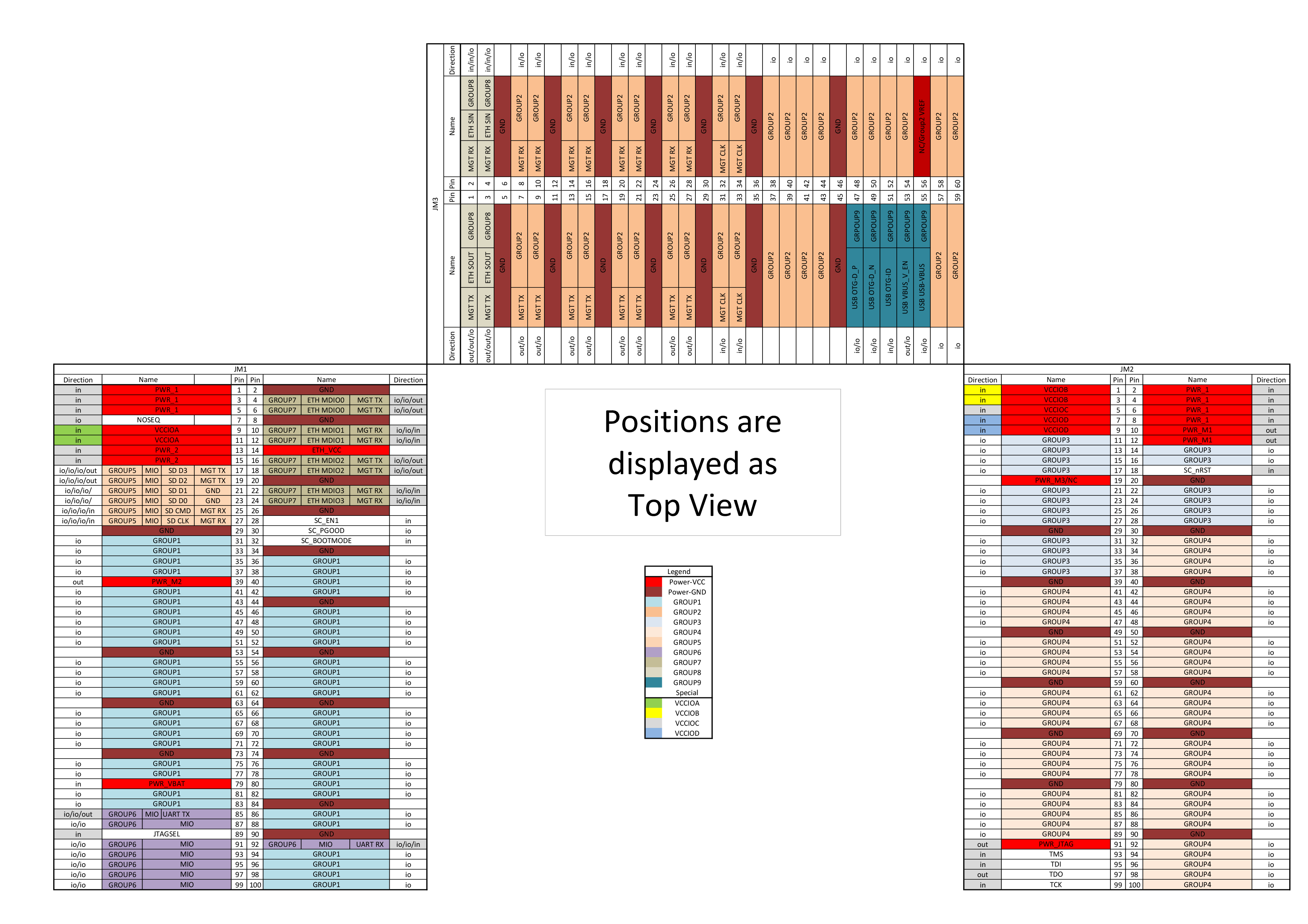 Image Removed Image Removed
|
Carrier Board Power Connection Table
I/O resource comparison for all 4x5 modules. There are maximum 4 user supplied I/O voltages (VCCIOA, VCCIOB, VCCIOC and VCCIOD). Attention: Maximum supply voltage for HP banks is 1.8V. |
| Scroll Title |
|---|
| title | Module basic power and group pin assignment, recommended to verify with Schematics |
|---|
|
Image Added |
Carrier Board Power Connection Table
| Scroll Title |
|---|
| title | Power Pin Connection on different Carrierboards |
|---|
|
| Scroll Table Layout |
|---|
| orientation | landscape |
|---|
| sortDirection | ASC |
|---|
| repeatTableHeaders | default |
|---|
| sortByColumn | 1 |
|---|
| sortEnabled | false |
|---|
| cellHighlighting | true |
|---|
|
| IO Voltage | B2B Connector | Carrier Boards |
|---|
| Name | Direction* | JB1 | JB2 | TE0701 | TE0703 Rev01 - Rev04 | TE0703 Rev 05 | TE0705 | TE0706 | TEBA0841 | TEBA0841 REV01 |
|
| Pin | Pin | Schematic Name | Value,Option,Comp. | Schematic Name | Value,Option,Comp. | Schematic Name | Value,Option,Comp. | Schematic Name | Value,Option,Comp. | Schematic Name | Value,Option,Comp. | Schematic Name | Value,Option,Comp. | Schematic Name | Value,Option,Comp. | | PWR_1 | out | 2,4,6 | 1,3,5,7 | 5V0 | 5V | 3.3V | 3.3V | 3.3V | 3.3V | 5V0 | 5V | 3.3V | 3.3V | 3.3V | use ext. 3.3V power supply | 3.3V | use ext. 3.3V power supply | | VCCIOA | out | 10,12 |
| VIOTB | FMC_VADJ 2V5 3.3VOUT | VCCIO35 | R23→M3.3VOUT J1B-B1 | VCCIOA | J5→M3.3VOUT, M1.8VOUT R23→M3.3VOUT J1-B1 | VIOTB | FMC_VADJ 2V5 3.3VOUT | VCCIO35 | R20->M3.3VOUT/J6B-B32 | VCCIOA | J26→ M1.8VOUT, 2.5V, 3.3V_OUT J20-6,J20-45 | VCCIOA | J26→ M1.8VOUT, 2.5V, 3.3V_OUT
J20-6,J20-45 | | VCCIOD | out |
| 8,10 | VIOTB | FMC_VADJ 2V5 3.3VOUT | VCCIO13 | R26→M3.3VOUT J2B-B1 | VCCIOD | J10→M3.3VOUT, M1.8VOUT R26→M3.3VOUT J2B-B1 | VIOTB | FMC_VADJ 2V5 3.3VOUT | VCCIO13 | R22->M3.3VOUT/J6B-B1 | VCCIOD | J27→ M1.8VOUT, 2.5V, 3.3V_OUT J17-6,J17-45 | VCCIOD | J27→ M1.8VOUT, 2.5V, 3.3V_OUT J17-6,J17-45 | | PWR_2 | out | 14,16 |
| 3V3IN | 3.3V |
|
| Scroll Title |
|---|
| title | Power Pin Connection on different Carrierboards |
|---|
|
| IO Voltage | B2B Connector | Carrier Boards |
|---|
| Name | Direction* | JB1 | JB2 | TE0701 | TE0703 Rev 01 - Rev 04 | TE0703 Rev 05 | TE0705 | TE0706 | TEBA0841 REV02 | | | | Pin | Pin | Schematic Name | Value,Option,Comp. | Schematic Name | Value,Option,Comp. | Schematic Name | Value,Option,Comp. | Schematic Name | Value,Option,Comp. | Schematic Name | Value,Option,Comp. | Schematic Name | Value,Option,Comp. | | PWR_1 | out | 2,4,6 | 1,3,5,7 | 5V0 | 5V | 3.3V | 3.3V | 3.3V | 3.3V | 5V03V3IN | 5V | 3.3V | 3.3V | 3.3V | 3.3V | use ext. 3.3V power supply | 3.3V | use ext. 3.3V power supply | VCCIOA | VCCIOB | out |
| 102,12 | | 4 | VIOTBno name / VIOTA
| FMC_VADJ 2V5 3.3VOUT | VCCIO35VCCIO34 | R23→M3J5→M3.3VOUT J1B-B1B32 | VCCIOAVCCIOB | J5→M3J8→M3.3VOUT,M1.8VOUT R23→M3.3VOUT J1-B1J2B-B32 | VIOTB | FMC_VADJ 2V5 3.3VOUT | VCCIO35 | R20->M3.3VOUT/J6B-B32 | VCCIOA | 1.8V | 1.8V | VCCIOB | J5→ J26→ M1.8VOUT, 2.5V, 3.3V_OUT
J20-6,J20-45 | VCCIOB | NC | | VCCIOC | VCCIOD | out | | 8,10 |
| 6 | VIOTBno name / VIOTA
| FMC_VADJ 2V5 3.3VOUT | VCCIO13VCCIO33 | R26→M3R25→M3.3VOUT J2B-B1B32 | VCCIODVCCIOC | J10→M3J9→M3.3VOUT, M1.8VOUT R26→M3R25→M3.3VOUT J2B-B1B32 | VIOTB | FMC_VADJ 2V5 3.3VOUT | VCCIO13VCCIO33 | R22R21->M3.3VOUT/J6B-B1 | VCCIODVCCIOC | J27→ J6→ M1.8VOUT, 2.5V, 3.3V_OUT | VCCIOC | NCJ17-6,J17-45 | | PWR_2M1 | outin | 14,16 | |
| 9,11 | 3.3VOUT | 3.3V | 3.3VOUT3V3IN | 3.3V | M3.3VOUT | 3.3V | 3.3VOUT | 3.3V | M3.3VOUT | 3.3V | 3.3V_OUT | 3V3IN | 3.3V | 3.3V_OUT | 3.3V | | PWR_M2 | in | VCCIOB40 |
| outVIOB | | 2,4 | no name / VIOTA
| FMC_VADJ 2V5 3.3VOUT | VCCIO34 | J5→M3.3VOUT J1B-B32 | VCCIOB | J8→M3.3VOUT,M1.8VOUT J2B-B32 | VIOTB | FMC_VADJ 2V5 3.3VOUT | 1.8V | 1.8V | VCCIOB | NC | | VCCIOC | out | | 6 | no name / VIOTA
| FMC_VADJ 2V5 3.3VOUT | VCCIO33 | R25→M3.3VOUT J2B-B32 | VCCIOC | J9→M3.3VOUT, M1.8VOUT R25→M3.3VOUT J2B-B32 | VIOTB | FMC_VADJ 2V5 3.3VOUT | VCCIO33 | R21->M3.3VOUT | VCCIOC | NC | | PWR_M1 | in | | 9,11 | 3.3VOUT | 3.3V | 3.3VOUT | 3.3V | M3.3VOUT | 3.3V | 3.3VOUT | 3.3V | M3.3VOUT | 3.3V | 3.3V_OUT | 3.3V | | PWR_M2 | in | 40 | | VIOB | 1.8V | M1.8VOUT | 1.8V | M1.8VOUT | 1.8V | VIOB | 1.8V | M1.8VOUT | 1.8V | M1.8VOUT | 1.8V | | PWR_M3 | in | | 20 | NC | | NC | | NC | | NC | | NC | | | NC | | PWR_VBAT | out | 80 | | VBAT | B1 | VBAT | J7 | VBAT | J7 | NC | | VBAT | J9 | VBAT | NC | | in | | 92 | VCCJTAG | | VCCJTAG | | VCCJTAG | | VCCJTAG | | VCCJTAG | | VCCJTAG | NC |
|
Power comparison of all 4x5 carrier boards. *Power direction based on carrier boards view.There are 4 variable user supplied I/O voltages (VCCIOA, VCCIOB, VCCIOC and VCCIOD). PWR_1 and PWR_2 are fixed from carrier boards. PWR_M1 and PWR_M2 normally use default value from module. NC=Not Connected
Attention: On some carrier boards the user supplied I/O voltages are connected together (red colored schematic names).
...
| title | Carrierboard basic power and group pin assignment (Top View), recommended to verify with Schematics |
|---|
| 1.8V | M1.8VOUT | 1.8V | M1.8VOUT | 1.8V | VIOB | 1.8V | M1.8VOUT | 1.8V | M1.8VOUT | 1.8V | M1.8VOUT | 1.8V | | PWR_M3 | in |
| 20 | NC |
| NC |
| NC |
| NC |
| NC |
|
| NC |
| NC | | PWR_VBAT | out | 80 |
| VBAT | B1 | VBAT | J7 | VBAT | J7 | NC |
| VBAT | J9 | VBAT | NC | VBAT | NC | | in |
| 92 | VCCJTAG |
| VCCJTAG |
| VCCJTAG |
| VCCJTAG |
| VCCJTAG |
| VCCJTAG |
| VCCJTAG | NC |
Power comparison of all 4x5 carrier boards. *Power direction based on carrier boards view.There are 4 variable user supplied I/O voltages (VCCIOA, VCCIOB, VCCIOC and VCCIOD). PWR_1 and PWR_2 are fixed from carrier boards. PWR_M1 and PWR_M2 normally use default value from module. NC=Not Connected Attention: On some carrier boards the user supplied I/O voltages are connected together (red colored schematic names). |
| Scroll Title |
|---|
| title | Carrierboard basic power and group pin assignment (Top View), recommended to verify with Schematics |
|---|
|
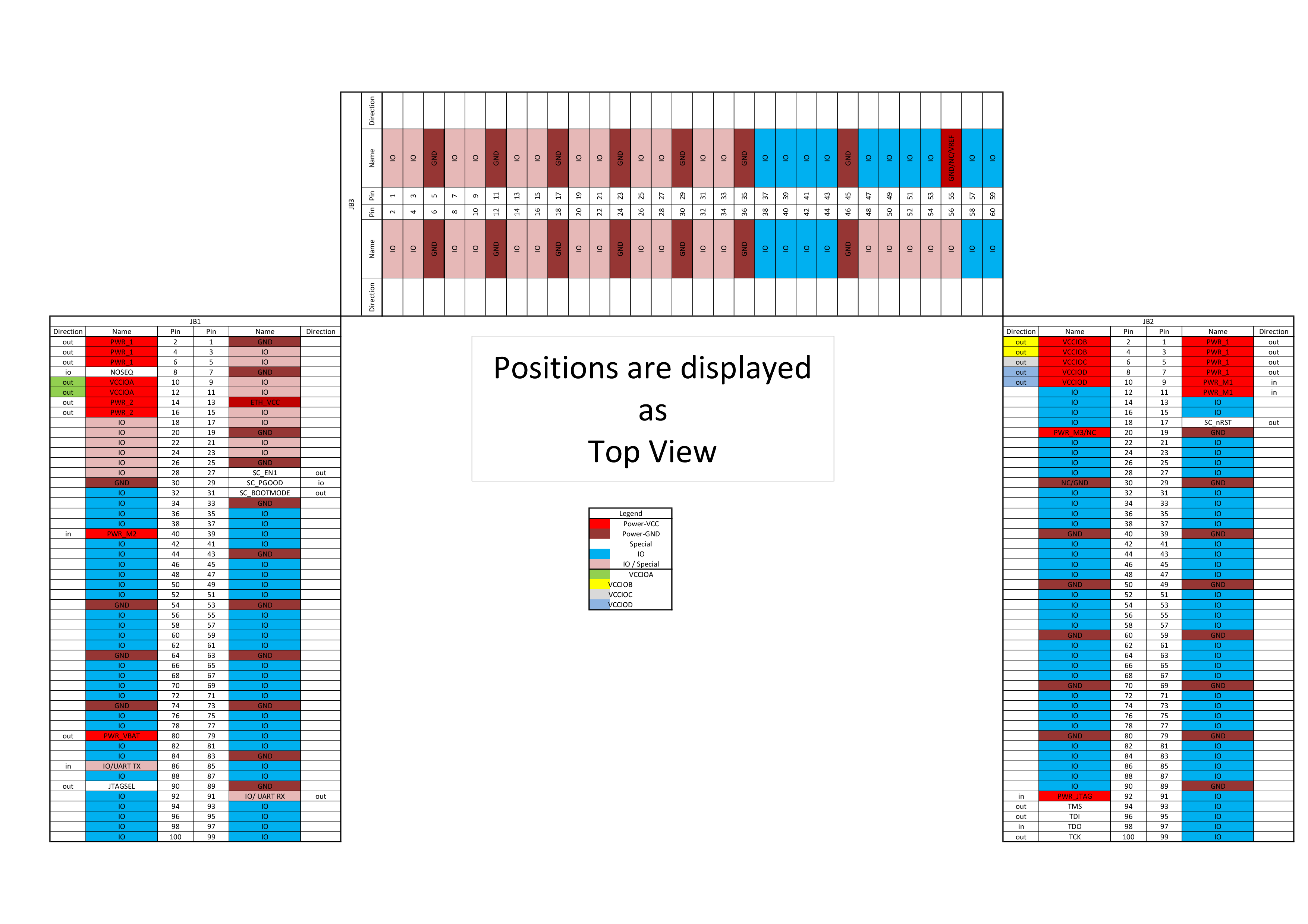 Image Added Image Added
|
4x5 Module Controller IOs
| Scroll Title |
|---|
| title | 4x5 Module Controller IOs |
|---|
|
| Scroll Table Layout |
|---|
| orientation | landscape |
|---|
| sortDirection | ASC |
|---|
| repeatTableHeaders | default |
|---|
| sortByColumn | 1 |
|---|
| sortEnabled | false |
|---|
| cellHighlighting | true |
|---|
|
| Name | Module B2B Pin | Carrier B2B Pin | Direction (Module view) | Description | Recommendation |
|---|
| JTAGSEL | JM1-89 | JB1-90 | in | JTAG Chain multiplexer. Low FPGA, High CPLD. For module with CPLD only. | Connect Pulldown on carrier.
DIP switch possible. | | SC_EN1 | JM1-28 | JB1-27 | in | Module power. Set high to enable module power. Note: Power management depends on module. Sometimes this is a only used as Power ON Reset like SC_nRST | Connect Pullup on carrier.
DIP switch possible | | SC_NOSEQ | JM1-7 | JB1-8 | in / inout | Module Power management. Set high to disable CPLD power management. Note: Power management depends on module and not all modules support extended power management with CPLD. | Connect Pullup on carrier.
DIP switch possible. | | SC_PGOOD | JM1-30 | JB1-29 | out / inout | Power Good signal. Is Low, if SC_EN1 is set to zero or if power is not ready, otherwise high impedance output. Note: Power management depends on module. | Connect Pullup on carrier.
Do not use this signal to enable FPGA Bank voltages. It's only for monitoring. To Enable FPGA Banks, use 3.3V(PWR_M1) or 1.8V(PWR_M2) module output. | | SC_BOOTMODE | JM1-32 | JB1-31 | in | Boot Mode selection Pin for Zynq module only. Default low for primary SD boot and high for primary QSPI boot. Note: Depends also on module CPLD firmware | Connect Pullup on carrier.
DIP switch possible. | | SC_nRST | JM2-18 | JB2-17 | in | Low active module reset. Pin force Power one reset on FPGA/SoC. Note: Depending from module CPLD or voltage supervisor is used. | Connect Pullup on carrier.
DIP switch possible. |
|
Remove 4x5 module
| Widget Connector |
|---|
| url | https://www.youtube.com/watch?v=uisv2dWbktc |
|---|
|
...
Compatibility Guide
Ethernet LED'S
...
Carrier Board Checklist
Schematic Checklist
...
|
|
|
|---|
| 1 | Are B2B pin numbers on the connectors mirrored compared to the module pin numbers? | As B2B connectors are "unisex" type the do mirror pin numbers when connecting. That is pin1 connects to pin2, and pin2 to pin1, etc. |
| 2 | Are B2B connectors named JB1, JB2, JB3? | This is not a hard requirement, but it helps to use the same identifiers. |
| 3 | Are all GND pins connected to a common ground net? |
|
| 4 | Are all VIN pins connected together? | |
|
| 5 | Is JB2 pin 92 pin used as VREF for the JTAG interface? | for future compatibility only, currently all modules have 3.3V JTAG |
| 6 | Are external circuits/buffers connecting to MIO bank 1 pins powered from JB1 pin 40? | JB1 pins 18, 20, 22, 24, 26, 28 use voltage at pin 40 as VCCIO. Currently it is 1.8V for all released modules. |
PCB Checklist
...
|
|
|
|---|
| | 1 | Are mounting holes placed properly? | Four Mounting holes should always be used. They are required for mounting screws and for module extraction. The mounting holes will also help in dissipating some heat from the module to the carried board PCB. Four holes with a 3.2mm diameter should be placed exactly at the corners of a 34mm by 44mm rectangle. |
|---|
| 2 | Are B2B headers properly placed? | B2B headers must be placed and aligned very precisely or the module will not align correctly (in the worst case module insertion could destroy the connectors or the PCB). The B2B headers should be locked on the PCB, and it is recommended that the position and placement be checked against placement dimensions before submitting the PCB files. |
| 3 | Are B2B headers rotated properly? | As B2B header pin numbers differ from module to the carrier (swap of odd and even numbers), it is recommended that that the rotation is checked in the PCB design. |
| 4 | Height clearance below module | Components can be placed below the module but height clearance rules must be obeyed. |
| 5 | Power dissipation of components below module | It is not recommended to place any components with high power dissipation below the module, as there will be almost no airflow below the module. |
...
| Note |
|---|
This placement is same for all 4x5 Modules! |
...
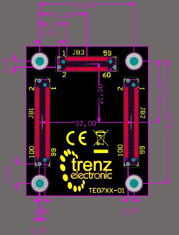
Top view of the Carrier Board.
Connector numbers as on base! (pin JB1.1 on base would mate to pin JM1.2 on module).