Page History
...
| Schematic net name | Default function | Direction | SC pin | FPGA pin | Description | |||
|---|---|---|---|---|---|---|---|---|
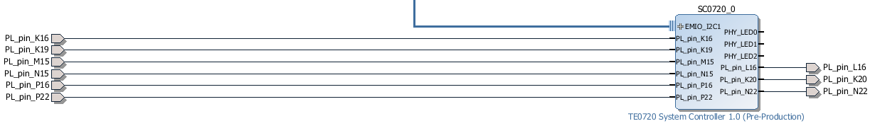
| XCLK | ETH PHY Clock to FPGA | to FPGA | K1 | K19 | ||||
| X1 | I2C Clock from FPGA | from FPGA | F1 | L16 | SCL from EMIO I2Cx | |||
| X7 | I2C Data from FPGA | from FPGA | M1 | N22 | SDA from EMIO I2Cx | |||
| X5 | I2C Data to FPGA | to FPGA | J1 | P22 | SDA to EMIO I2Cx | |||
| X2 | ETH PHY LED1LED0 | to FPGA | C2 | M15 | ||||
| X4 | ETH PHY LED2 | to FPGA | D1 | P16 | ||||
| X3Interrupt | ETH PHY LED1 | to FPGA | B1 | N15 | RTC, MEMS Interrupt or PHY LED3LED1 | |||
| X0 | - | - | not used on TE0720-02 | |||||
| PUDC | K16 | normally not used tied to fixed level by SC |
It is recommended to use Vivado IP Core available for 2014.2 and later versions.
...
| Pin/Function | Used as/Mapped to | Notes | ||
|---|---|---|---|---|
| ETH PHY LED0 | XIO to FPGA | |||
| ETH PHY LED1 | XIO to FPGA | |||
| ETH PHY LED2 | Not used | XIO to FPGA | ||
| ETH PHY CONFIG | Tied logic low | PHY Address set to 0 | ||
| ETH CLK125MHz | Pass through FPGA B34 SRCC pin | |||
| ETH Clock Enable | Tied logic high | |||
| ETH PHY Reset | Internal RESET | |||
| MIO7 | LED1 | |||
| MEMS/RTC I2C | XIO to FPGA | |||
| RTC Interrupt | - | |||
| MEMS Interrupt 1 | - | |||
| MEMS Interrupt 2 | - | |||
| eMMC Reset | Internal RESET | |||
| USB PHY Reset | Internal RESET | |||
| FPGA PUDC | Tied logic low | |||
| FPGA PROG_B | Tied logic high | |||
| Zynq Cascaded JTAG | Enabled (pulled low) | |||
| Zynq boot mode | SPI or SD, depending on bootmode pin | |||
| Zynq SRST | Tied logic high | |||
| Zynq POR | Internal POR/Reset | |||
| PLL | Not used | |||
| LED2 | System Status LED | |||
| LED1 | MIO7 | |||
| NOSEQ Input | NOSEQ at power, LED out after boot | |||
| Power Good 1.5V | ||||
| Power Good VTT | ||||
| MODE Input |
| I2C Address | Function | ||
|---|---|---|---|
| 0x20 | Status reg 1 | ||
| 0x21 | Status reg 2 |
LED Control Status
The TE0720 on-board LED devices can be remapped to different functions.
...
| Addr | R/W | Register name | Descripion | ||
|---|---|---|---|---|---|
| 0 | RO | ||||
| 1 | RO | ||||
| 2 | RO | ID1 | Identifier Register 1 | ||
| 3 | RO | ID2 | Identifier Register 2 | ||
| 4 | RO | ID3 | Identifier Register 3 | ||
| 5 | RW | CR1 | Control Register 1: LED's | ||
| 6 | RW | CR2 | Control Register 2; XIO Control | ||
| 7 | RW | CR3 | Control Register 3; Reset, Interrupt | ||
| 8 | RO | SR1 | Status Register | ||
| 9 | RO | MAChi | Highest bytes of primary MAC Address | ||
| 0xA | RO | MACmi | Middle bytes of primary MAC Address | ||
| 0xB | RO | MAClo | Lowest bytes of primary MAC Address | ||
| 0xC | CR4 | reserved do not use | |||
| 0xD | RW | MMD_CR | MMD Control Register | ||
| 0xE | RW | MMD_AD | MMD Address/Data | ||
| 0xF | - | reserved do no use | |||
| other | - | reserved do not use |
Register CR1
| Bit | Description |
|---|---|
| 15:12 | - |
| 11:8 | Noseq MUX |
| 7:4 | LED2 MUX |
| 3:0 | LED1 MUX |
| Value | LED1 | LED2 | NOSEQ | ||||
|---|---|---|---|---|---|---|---|
| Default | MIO7 | Mode Blink | PHY_LED0 | ||||
| 0001 | PHY_LED0 | PHY_LED0 | PHY_LED0 | ||||
| 0010 | PHY_LED1 | PHY_LED1 | PHY_LED1 | ||||
| 0011 | PHY_LED2 | PHY_LED2 | PHY_LED2 | ||||
| 0100 | MIO7 | MIO7 | MIO7 | ||||
| 0101 | RTC_INT | RTC_INT | RTC_INT | ||||
| 0110 | OFF | OFF | OFF | ||||
| 0111 | ON | ON | ON | ||||
| 1000 | MIO14/MIO15 | MIO14/MIO15 | REV 05, UART activity | ||||
| 1001 | MIO14 | MIO15 | REV 05 | ||||
| 1010 | REV 05 |
...
Register CR2
| Bit | Description |
|---|---|
| 15:12 | XCLK select |
| 11:8 | XIO6 select |
| 7:4 | XIO5 select |
| 3:0 | XIO4 select |
Signal XIO4
| XIO4 select | Signal out value |
|---|---|
| "0001" | MIO7 |
| "0010" | SHA_IO |
| "0011" | MAC_IO |
| "0110" | 'Z' (Configured as input) |
| all others | PHY_LED0 |
Signal XIO5
| XIO5 select | Signal out value |
|---|---|
| "0101" | RTC_INT |
| "0110" | 'Z' (Configured as input) |
| all others | PHY_LED1 |
...
Signal XIO6
| XIO6 select | Signal out value |
|---|---|
| "0110" | 'Z' (Configured as input) |
| "0111" | INTR |
| all others | PHY_LED2 |
Signal XCLK
| XCLK Select | Signal out value |
|---|---|
| "0001" | RTC_INT |
| "0010" | Internal Oscillator Out ~24.18 MHz |
| all others | 125 MHz |
...
Signal SHA_IO
| XIO4 select | Signal out value |
|---|---|
| "0010" | XIO5 |
| all others | 'Z' (Configured as input) |
...
Signal MAC_IO
| XIO4 Select | Signal out value |
|---|---|
| "0011" | XIO5 |
| all others | Connected to internal MAC read block |
...
System Controller version 0.02 does not support extended address space - registers 0xD and 0xE are read-write accessible but do not have any function. In feature revision extended address will be used to control SC PLL and other features.
...
Interrupt can be selected instead of PHY_LED2 on XIO6 pin, by setting CR2 bits 11 downto 8 to "0111"
Overview: On-board LEDs
There are 3 on-board LEDs, with two of them connected to the System Management Controller and one to the Zynq PL (Done pin).
| Name | Color | Connected to: | Default mapping: |
|---|---|---|---|
| LED1 | Green | SC | PL MIO[7] |
| LED2 | Red | SC | System Controller Status LED |
| LED3 | Green | Zynq PL | FPGA Done - active low |
LED1 GREEN
Is mapped to MIO7 after power up. After the Zynq PS has booted it can change the mapping of this LED. If SC can not enable power to the Zynq then this LED will remain under SC control. It is available to the user only after the power supplies have stabilized and the POR reset to the Zynq is released.
...
| Note |
|---|
| This LED will not operate if the SC can not power on the 3.3V output rail that also powers the 3.3V circuitry on the module. |
LED Status Codes
| # | GLED1 | RLED2 | GLED3 | Status | Description |
|---|---|---|---|---|---|
| 1 | OFF | OFF | ON | Fatal power error | This combination after power up is only possible in no sequencing compatibility mode were 3.3Vout is supplied externally. The 1.0V and 1.8V DC-DC supplies are forced on (NOSEQ=1), and the SC is not able to start (3.3Vin below 2.1V). This should never happen if the external power supplies are OK. |
| 2 | OFF | ON | OFF | VIN missing (or EN1 low) | 3.3Vin is present, but the DC-DC supplies are not powered or 3.3Vin is below 3.05V. If the LEDs stay on in this state then 3.3Vout is not turned on, and the Zynq is kept in the POR state. |
| 3 | OFF | 1/2 Blink Fast 4 Hz | ON | OK | Boot mode selected is SPI Flash. This status remains after boot also if the LED settings are not changed and user is not controlling MIO7 and FPGA is not loaded. |
| 4 | OFF | 1/2 Blink Slow 1 Hz | ON | OK | Boot mode selected is SD Card. This status remains after boot also if the LED settings are not changed and user is not controlling MIO7 and FPGA is not loaded. |
| 5 | MIO7 or user function | Blink or user function | OFF | OK | LED3 goes off when the FPGA is configured. NOTE: The FPGA design can control this LED too using STARTUPE2, so it may remain ON or be flashing when the FPGA is configured. |
| 6 | ON | Slow blink 0.5Hz, 1/8 on, 7/8 off | OFF | Powerdown | EN1 input to the module is low. If sequencing is enabled in this mode, then all power supplies on the module are OFF. |
| 7 | ON | Slow blink 0.5Hz, 1/8 on, 7/8 off | ON |
| EN1 input to the module is low. Sequencing is disabled module is in reset state. | |||||
| 8 | ON | ON | ON | Reset | Powered, RESIN input is active low or Bank B34 Supply Voltage is missing. |
...
If green LED3 does not light up at least for short time at power then there is major problem with power supplies, FPGA core and aux voltages may be missing.
| HTML |
|---|
<!-- |
Overview
Firmware for PCB CPLD with designator U19. CPLD Device in Chain: LCMX02-1200HC
...
Overview
Content Tools