...
| Page properties |
|---|
|
Template Revision 2.6
- Module: TRM Name always "TE Series Name" +TRM
Example: "TE0728 TRM" - Carrier: TRM Name usually "TEB Series Name" +TRM
Example: "TEB0728 TRM"
|
...
| Page properties |
|---|
|
Important General Note:
|
...
| Page properties |
|---|
|
Note for Download Link of the Scroll ignore macro: |
...
...
Intel® MAX 10 Commercial [10M08SAU169C8G]
SDRAM Memory up to 64Mb, 166MHz
Dual High Speed USB to Multipurpose UART/FIFO IC
Quad SPI Flash, 64Mb
EEPROM Memory, 4Kb
8x User LED
Micro USB2 Receptacle 90
18 Bit 2MSPS Analog to Digital Converter
2x SMA Female Connector
I/O interface:
Power Supply:
Dimension: 86.5mm x 25mm
Others:
Block Diagram
| Page properties |
|---|
|
add drawIO object here.
|
...
| Scroll Title |
|---|
| anchor | Figure_OV_BD |
|---|
| title | TEI0015 main components |
|---|
|
| Scroll Ignore |
|---|
| draw.io Diagram |
|---|
| border | false |
|---|
| viewerToolbar | true |
|---|
| |
|---|
| fitWindow | false |
|---|
| diagramDisplayName | |
|---|
| lbox | true |
|---|
| revision | 13 |
|---|
| diagramName | TEI0015_OV_MC |
|---|
| simpleViewer | false |
|---|
| width | |
|---|
| links | auto |
|---|
| tbstyle | hidden |
|---|
| diagramWidth | 641 |
|---|
|
|
| Scroll Only |
|---|
|
|
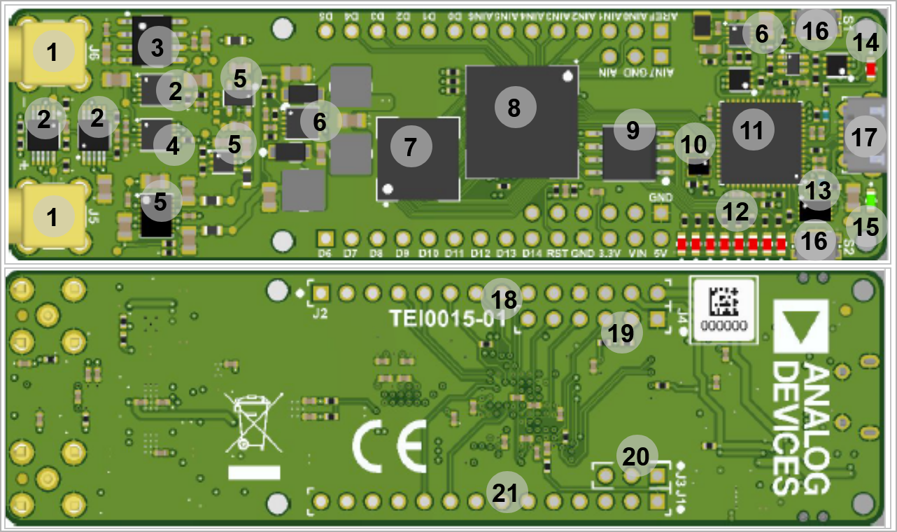
SMA Connector, J5...6
Amplifier, U12- U14- U6
Series Voltage Reference, U8
Analog to Digital Convertor, U15
Voltage Regulator, U10- U13- U16
Switching Voltage Regulator, U11- U4
Intel® MAX 10, U1
SDRAM Memory, U2
SPI Flash Memory, U5
12.00 MHz MEMS oscillator, U7
FTDI USB2 to JTAG/UART adapter, U3
User LEDs, D2...9
4Kb EEPROM, U9
Configuration LED (Red) , D10
Power-on LED (Green), D1
Push button, S1...2
Micro USB2 Receptacle, J9
1x14 pin header (Not assembled), J2
1x6 pin header (Not assembled), J4
Jumper, J3
1x14 pin header (Not assembled), J1
Initial Delivery State
| Page properties |
|---|
|
Notes : Only components like EEPROM, QSPI flash and DDR3 can be initialized by default at manufacture. If there is no components which might have initial data ( possible on carrier) you must keep the table empty |
...
| Scroll Title |
|---|
| anchor | Table_OBP_USB |
|---|
| title | Micro USB-2 connector pins |
|---|
|
| Scroll Table Layout |
|---|
| orientation | portrait |
|---|
| sortDirection | ASC |
|---|
| repeatTableHeaders | default |
|---|
| style | |
|---|
| widths | |
|---|
| sortByColumn | 1 |
|---|
| sortEnabled | false |
|---|
| cellHighlighting | true |
|---|
|
| Pins | Connected to | Note |
|---|
| VBUS | USB_VBUS | It is connected to GND | | D+ | FTDI FT2232H U3, DP pin |
| | D- | FTDI FT2232H U3, DM pin |
|
|
JTAG Interface
JTAG access to the TEI0015 SoM through pin header connector J4.
| Scroll Title |
|---|
| anchor | Table_SIP_JTG |
|---|
| title | JTAG pins connection |
|---|
|
| Scroll Table Layout |
|---|
| orientation | portrait |
|---|
| sortDirection | ASC |
|---|
| repeatTableHeaders | default |
|---|
| style | |
|---|
| widths | |
|---|
| sortByColumn | 1 |
|---|
| sortEnabled | false |
|---|
| cellHighlighting | true |
|---|
|
JTAG Signal | Pin Header Connector | Note |
|---|
| TMS | J4-6 |
| | TDI | J4-5 |
| | TDO | J4-4 |
| | TCK | J4-3 |
| | JTAG_EN | J4-2 |
|
|
On-board Peripherals
| Page properties |
|---|
|
Notes : - add subsection for every component which is important for design, for example:
- Two 100 Mbit Ethernet Transciever PHY
- USB PHY
- Programmable Clock Generator
- Oscillators
- eMMCs
- RTC
- FTDI
- ...
- DIP-Switches
- Buttons
- LEDs
|
...
| Scroll Title |
|---|
| anchor | Table_OBP_SDRAM |
|---|
| title | SDRAM interface IOs and pins |
|---|
|
| Scroll Table Layout |
|---|
| orientation | portrait |
|---|
| sortDirection | ASC |
|---|
| repeatTableHeaders | default |
|---|
| style | |
|---|
| widths | |
|---|
| sortByColumn | 1 |
|---|
| sortEnabled | false |
|---|
| cellHighlighting | true |
|---|
|
| SDRAM I/O Signals | Signal Schematic Name | Connected to | Notes |
|---|
| Address inputs | A0 ... A13 | bank 3 | - | Bank address inputs
| BA0 / BA1 | bank 3 | - | | Data input/output | DQ0 ... DQ15 | bank 6 | - | | Data mask | DQM0 ... DQM1 | bank 6 | - | | Clock | CLK | bank 3 |
| | Control Signals | CS | bank 3 | Chip select | CKE | bank 3 | Clock enable | RAS | bank 3 | Row Address Strobe | CAS | bank 3 | Column Address Strobe | | WE | bank 3 | Write Enable |
|
FTDI FT2232H
The FTDI chip U3 converts signals from USB2 to a variety of standard serial and parallel interfaces. Refer to the FTDI data sheet to get information about the capacity of the FT2232H chip. FTDI FT2232H chip is used in MPPSE mode for JTAG, 6 I/O's of Channel B are routed to FPGA bank 8 of the FPGA SoC and are usable for example as GPIOs, UART or other standard interfaces.
...
| Scroll Title |
|---|
| anchor | Table_PWR_PR |
|---|
| title | Module power rails. |
|---|
|
| Scroll Table Layout |
|---|
| orientation | portrait |
|---|
| sortDirection | ASC |
|---|
| repeatTableHeaders | default |
|---|
| style | |
|---|
| widths | |
|---|
| sortByColumn | 1 |
|---|
| sortEnabled | false |
|---|
| cellHighlighting | true |
|---|
|
| Connector Designator | VCC / VCCIO Schematic Name | Voltage | Direction | Notes |
|---|
J2
| VIN | 5V | Input |
| | 3.3V | 3.3V | Output |
| | 5V | 5V | Output |
| J9 | USB_VBUS | 5V | Input |
|
|
Bank Voltages
| Scroll Title |
|---|
| anchor | Table_PWR_BV |
|---|
| title | Zynq SoC bank voltages. |
|---|
|
| Scroll Table Layout |
|---|
| orientation | portrait |
|---|
| sortDirection | ASC |
|---|
| repeatTableHeaders | default |
|---|
| style | |
|---|
| widths | |
|---|
| sortByColumn | 1 |
|---|
| sortEnabled | false |
|---|
| cellHighlighting | true |
|---|
|
| Schematic Name | | Notes |
|---|
| Bank 1A | VCCIO1A | 3.3V |
| | Bank 1B | VCCIO1B | 3.3V |
| | Bank 2 | VCCIO2 | 3.3V |
| | Bank 3 | VCCIO3 | 3.3V |
| | Bank 5 | VCCIO5 | 3.3V |
| | Bank 6 | VCCIO6 | 3.3V |
| | Bank 8 | VCCIO8 | 3.3V |
|
|
...
| Scroll Title |
|---|
| anchor | Table_TS_AMR |
|---|
| title | Absolute maximum ratings |
|---|
|
| Scroll Table Layout |
|---|
| orientation | portrait |
|---|
| sortDirection | ASC |
|---|
| repeatTableHeaders | default |
|---|
| style | |
|---|
| widths | |
|---|
| sortByColumn | 1 |
|---|
| sortEnabled | false |
|---|
| cellHighlighting | true |
|---|
|
| Symbols | Description | Min | Max | Unit | Reference Document |
|---|
VIN | Supply voltage | 4.75 | 5.25 | V |
| | VCC_ONE | Supply voltage for core and periphery through on-die voltage
regulator | -0.5 | 3.9 | V | Intel MAX 10 datasheet | | VCCIO | Supply voltage for input and output buffers | -0.5 | 3.9 |
| Intel MAX 10 datasheet | | VCCA | Supply voltage for phase-locked loop (PLL) regulator and ADC | -0.5 | 3.9 |
| Intel MAX 10 datasheet | | V_AN_IN | Analog Input Voltage on ADC IC U15 pins | –0.3 | 5.4 | V | AD4003BCPZ datasheet | | V_REF | Analog reference voltage on IC U15 | -0.3 | 6 | V | AD4003BCPZ datasheet | T_STG | Storage Temperature | -25 | +85 | °C |
|
|
...
| Scroll Title |
|---|
| anchor | Table_TS_ROC |
|---|
| title | Recommended operating conditions. |
|---|
|
| Scroll Table Layout |
|---|
| orientation | portrait |
|---|
| sortDirection | ASC |
|---|
| repeatTableHeaders | default |
|---|
| style | |
|---|
| widths | |
|---|
| sortByColumn | 1 |
|---|
| sortEnabled | false |
|---|
| cellHighlighting | true |
|---|
|
| Symbols | Min | Max | Unit | Reference Document |
|---|
VIN supply voltage (5.0V nominal) | 4.75 | 5.25 | V |
| | VCC_ONE | 3.135 | 3.456 | V | see Intel MAX 10 datasheet | | VCCIO | 3.135 | 3.456 | V | see Intel MAX 10 datasheet | | VCCA | 3.135 | 3.456 | V | see Intel MAX 10 datasheet | | V_AN_IN | -0.1 | 5.1 | V | see AD4003BCPZ datasheet | | V_REF | 2.4 | 5.1 | V | see AD4003BCPZ datasheet | T_OP | 0 | +70 | °C | W9864G6JT-6 datasheet |
|
...