...
Intel® MAX 10 Commercial [10M08SAU169C8G]
SDRAM Memory up to 64Mb, 166MHz
Dual High Speed USB to Multipurpose UART/FIFO IC
64 Mb Quad SPI Flash
4Kb EEPROM Memory
8x User LED
Micro USB2 Receptacle 90
18 Bit 2MSPS Analog to Digital Converter
2x SMA Female Connector
I/O interface: 23x GPIO
Power Supply:
Dimension: 86.5mm x 25mm
Others:
...
| Scroll Title |
|---|
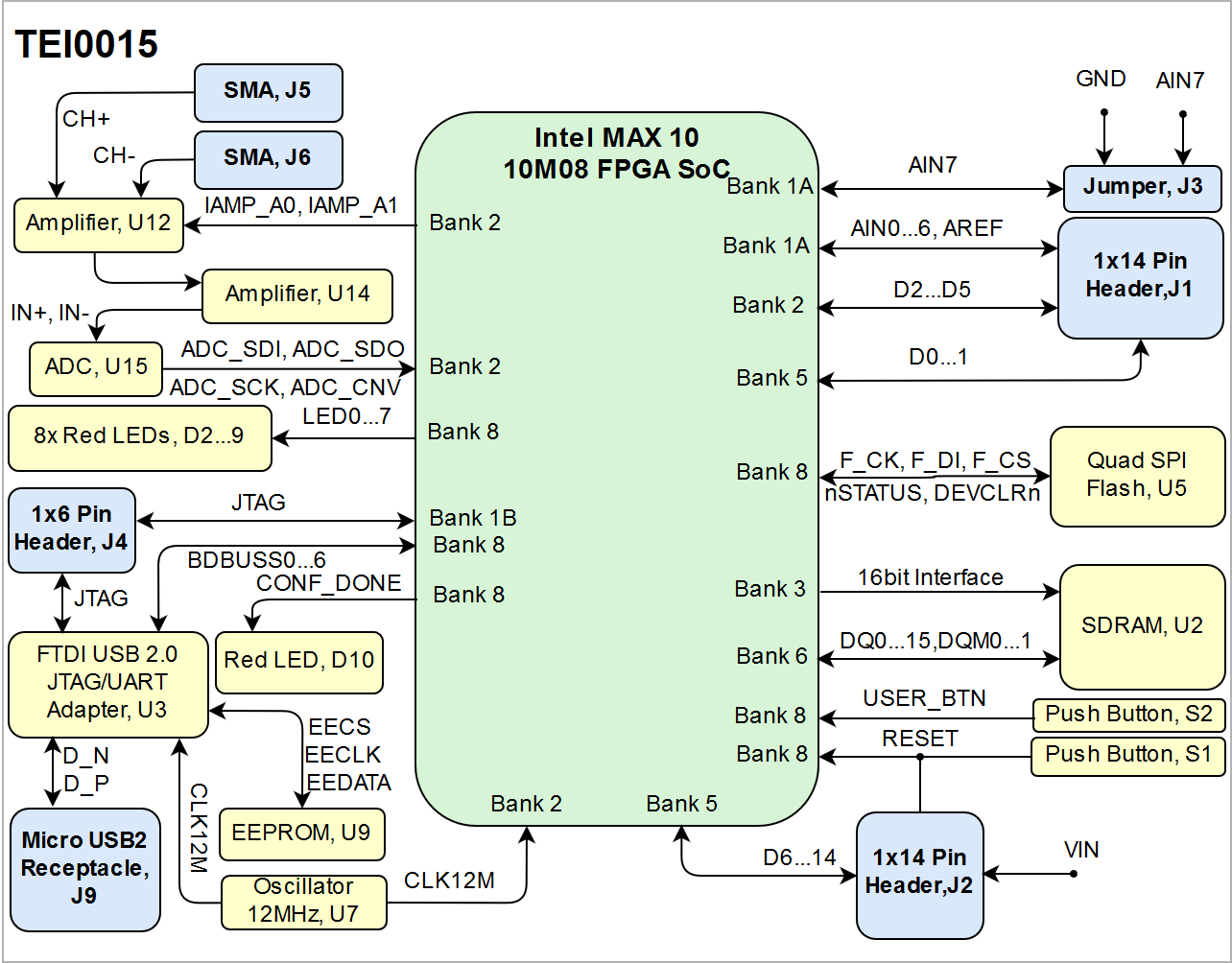
| anchor | Figure_OV_BD |
|---|
| title | TEI0015 block diagram |
|---|
|
| Scroll Ignore |
|---|
| draw.io Diagram |
|---|
| border | false |
|---|
| viewerToolbar | true |
|---|
| |
|---|
| fitWindow | false |
|---|
| diagramDisplayName | |
|---|
| lbox | true |
|---|
| revision | 2327 |
|---|
| diagramName | TEI0015_OV_BD |
|---|
| simpleViewer | false |
|---|
| width | |
|---|
| links | auto |
|---|
| tbstyle | hidden |
|---|
| diagramWidth | 643642 |
|---|
|
|
| Scroll Only |
|---|
|
|
Main Components
...
SMA Connector, J5...6
Amplifier, U12 - U14 - U6
Series Voltage Reference, U8
Analog to Digital ConvertorConverter, U15
Voltage Regulator, U10 - U13 - U16
Switching Voltage Regulator, U11 - U4
SDRAM Memory, U2
- Intel® MAX 10, U1
Active serial SPI Flash Memory, U5
12.00 MHz MEMS oscillator, U7
FTDI USB2 to JTAG/UART adapter, U3
User LEDs, D2...9
4Kb EEPROM, U9
Configuration LED (Red) , D10
Power-on LED (Green), D1
Push button, S1...2
Micro USB2 Receptacle, J9
1x14 pin header header, J2 (Not assembled), J2
1x6 pin header header, J4 (Not assembled), J4
Jumper, J3
1x14 pin header header, J1 (Not assembled), J1
Initial Delivery State
| Page properties |
|---|
|
Notes : Only components like EEPROM, QSPI flash and DDR3 can be initialized by default at manufacture. If there is no components which might have initial data ( possible on carrier) you must keep the table empty |
...
| Scroll Title |
|---|
| anchor | Table_OBP_IOs |
|---|
| title | FPGA I/O Banks |
|---|
|
| FPGA Bank | I/O Signal Count | Connected to | Notes |
|---|
| Bank 1A | 7 | 1x14 Pin header, J1 | AIN0...6 | | 1 | Jumper, J3 | AIN7 | | Bank 1B | 5 | 1x6 Pin header, J4 | JTAG_EN, TDI, TDO, TMS, TCK | Bank 2
| 4 | 1x14 Pin header, J1 | D2...5 | | 5 | A2D, U15 | ADC_EN, ADC_SDI, ADC_SDO, ADC_SCK, ADC_CNV | | 1 | 12MHz Oscillator, U7 | CLK12M | | 2 | Amplifier, U12 | nIAMP_A0, nIAMP_A1 | | Bank 3 | 22 | SDRAM, U2 | RAM_ADDR_CMD | | Bank 5 | 9 | 1x14 Pin header, J2 | DIO6...14 | | 2 | 1x14 Pin header, J1 | DIO0...1 | | 1 | D12_R | DIO12 | | Bank 6 | 16 | SDRAM, U2 | DQ0...15 | | 2 | SDRAM, U2 | DQM0...1 | | 1 | D11_R | DIO11 | Bank 8
| 8 | User Red LEDs, D2...9 | LED0...7 | | 6 | SPI Flash, U5 | F_CS, F_CKL, F_DI, F_DO, nSTATUS, DEVCLRn | | 1 | Red LED, D10 | CONF_DONE | | 6 | FTDI JTAG/UART Adapter, U3 | BDBUS0...5 | | 1 | Push Button, S2 | USER_BTN |
|
Micro-USB2
...
Connector
The Micro-USB2 connector J9 provides an interface to access the UART and JTAG functions via FTDI FT2232 chip. The use of this feature requires that USB driver is installed on your host PC.
| Scroll Title |
|---|
| anchor | Table_OBP_USB |
|---|
| title | Micro USB-2 connector pins |
|---|
|
| Scroll Table Layout |
|---|
| orientation | portrait |
|---|
| sortDirection | ASC |
|---|
| repeatTableHeaders | default |
|---|
| style | |
|---|
| widths | |
|---|
| sortByColumn | 1 |
|---|
| sortEnabled | false |
|---|
| cellHighlighting | true |
|---|
|
| Pins | Connected to | Note |
|---|
| VBUS | USB_VBUS | It is connected to GND |
| | D+ | FTDI FT2232H U3, DP pin |
| | D- | FTDI FT2232H U3, DM pin |
|
|
...
| Scroll Title |
|---|
| anchor | Table_SIP_JTG |
|---|
| title | JTAG pins connection |
|---|
|
| Scroll Table Layout |
|---|
| orientation | portrait |
|---|
| sortDirection | ASC |
|---|
| repeatTableHeaders | default |
|---|
| style | |
|---|
| widths | |
|---|
| sortByColumn | 1 |
|---|
| sortEnabled | false |
|---|
| cellHighlighting | true |
|---|
|
JTAG Signal | Pin Header Connector | Note |
|---|
| TMS | J4-6 |
| | TDI | J4-5 |
| | TDO | J4-4 |
| | TCK | J4-3 |
| | JTAG_EN | J4-2 | Connected Pulled-up to 3.3V |
|
On-board Peripherals
...
| Scroll Title |
|---|
| anchor | Table_OBP_SDRAM |
|---|
| title | SDRAM interface IOs and pins |
|---|
|
| Scroll Table Layout |
|---|
| orientation | portrait |
|---|
| sortDirection | ASC |
|---|
| repeatTableHeaders | default |
|---|
| style | |
|---|
| widths | |
|---|
| sortByColumn | 1 |
|---|
| sortEnabled | false |
|---|
| cellHighlighting | true |
|---|
|
| SDRAM I/O Signals | Signal Schematic Name | Connected to | Notes |
|---|
| Address inputs | A0 ... A13 | bank 3 | - | | Bank address inputs | BA0 / BA1 | bank 3 | - | | Data input/output | DQ0 ... DQ15 | bank 6 | - | | Data mask | DQM0 ... DQM1 | bank 6 | - | | Clock | CLK | bank 3 | - | | Control Signals | CS | bank 3 | Chip select | CKE | bank 3 | Clock enable | RAS | bank 3 | Row Address Strobe | CAS | bank 3 | Column Address Strobe | | WE | bank 3 | Write Enable |
|
...
| Scroll Title |
|---|
| anchor | Table_OBP_LED |
|---|
| title | On-board LEDs |
|---|
|
| Scroll Table Layout |
|---|
| orientation | portrait |
|---|
| sortDirection | ASC |
|---|
| repeatTableHeaders | default |
|---|
| style | |
|---|
| widths | |
|---|
| sortByColumn | 1 |
|---|
| sortEnabled | false |
|---|
| cellHighlighting | true |
|---|
|
| Designator | Color | Connected to | Active Level | Note |
|---|
| D2...9 | Red | LED1...8 | Active High | User LEDs | | D10 | Red | CONF_DONE | Active Low | Configuration DONE LED | | D1 | Green | 3.3V | Active High | After power on it will be on. |
|
Push Bottuns
| Scroll Title |
|---|
| anchor | Table_OBP_LED |
|---|
| title | On-board Push Buttons |
|---|
|
| Scroll Table Layout |
|---|
| orientation | portrait |
|---|
| sortDirection | ASC |
|---|
| repeatTableHeaders | default |
|---|
| style | |
|---|
| widths | |
|---|
| sortByColumn | 1 |
|---|
| sortEnabled | false |
|---|
| cellHighlighting | true |
|---|
|
| Designator | Connected to | Functionality | Note |
|---|
| S1 | RESET | General reset |
| | S2 | USER_BTN | User push button | Connected to FPGA Bank 8. |
|
Clock Sources
| Scroll Title |
|---|
| anchor | Table_OBP_CLK |
|---|
| title | Osillators |
|---|
|
| Scroll Table Layout |
|---|
| orientation | portrait |
|---|
| sortDirection | ASC |
|---|
| repeatTableHeaders | default |
|---|
| style | |
|---|
| widths | |
|---|
| sortByColumn | 1 |
|---|
| sortEnabled | false |
|---|
| cellHighlighting | true |
|---|
|
| Clock Source | Schematic Name | Frequency | Note |
|---|
| Microchip MEMS Oscillator, U7 | CLK12M | 12.00 MHz | Connected to FTDI FT2232 U3, pin 3. Connected to FPGA SoC bank 2, pin H6. |
|
Power and Power-On Sequence
...
| Scroll Title |
|---|
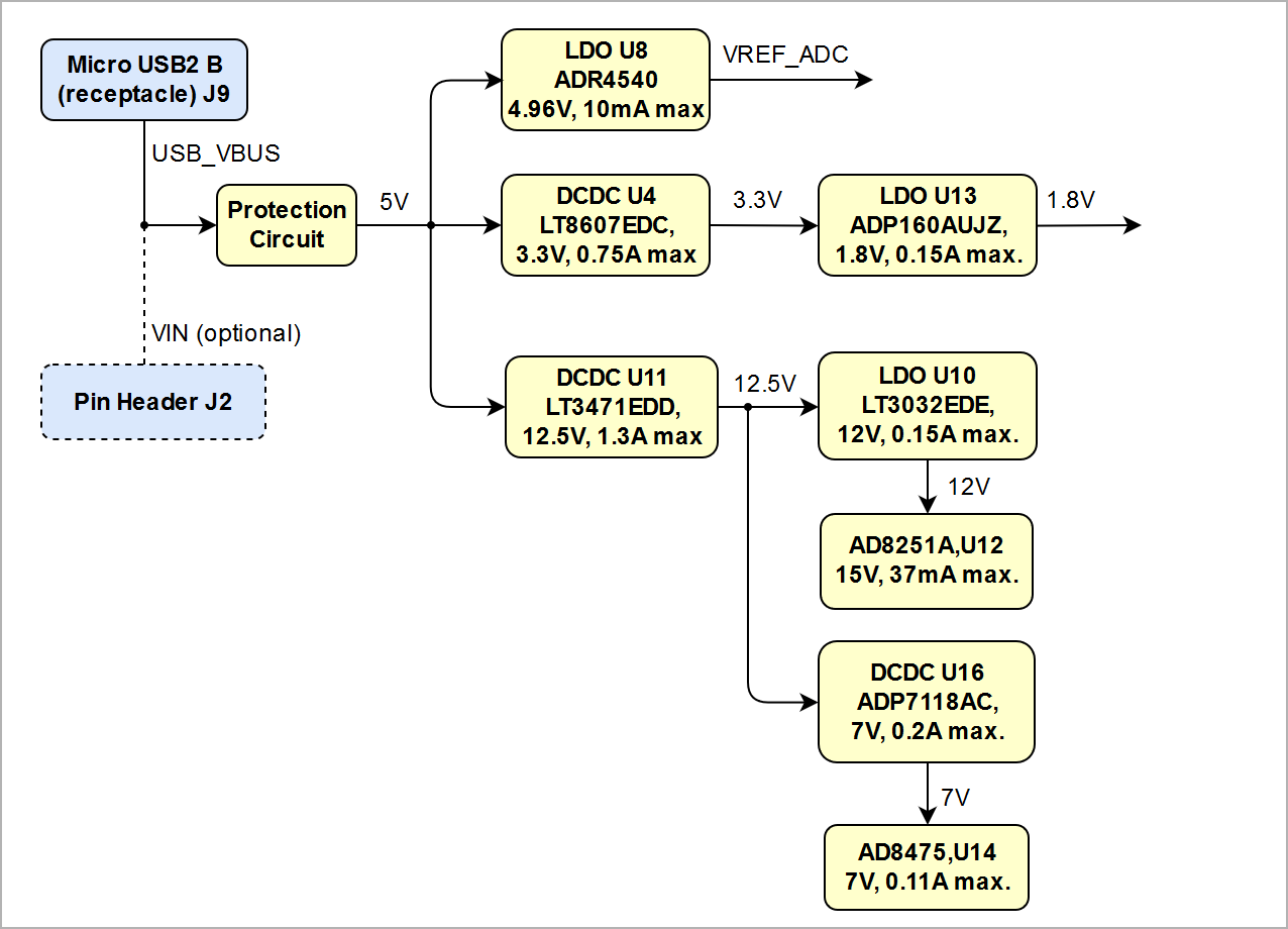
| anchor | Figure_PWR_PD |
|---|
| title | Power Distribution |
|---|
|
| Scroll Ignore |
|---|
| draw.io Diagram |
|---|
| border | false |
|---|
| viewerToolbar | true |
|---|
| |
|---|
| fitWindow | false |
|---|
| diagramDisplayName | TEI0015_PWR_P |
|---|
| lbox | true |
|---|
| revision | 1112 |
|---|
| diagramName | TEI0015_PWR_PD |
|---|
| simpleViewer | false |
|---|
| width | |
|---|
| links | auto |
|---|
| tbstyle | hidden |
|---|
| diagramWidth | 638 |
|---|
|
|
| Scroll Only |
|---|
|
|
...
There is no specific or special power-on sequence, just one single power source is needed. After power on the Green green LED (D1) will be on.
Power Rails
| Scroll Title |
|---|
| anchor | Table_PWR_PR |
|---|
| title | Module power rails. |
|---|
|
| Scroll Table Layout |
|---|
| orientation | portrait |
|---|
| sortDirection | ASC |
|---|
| repeatTableHeaders | default |
|---|
| style | |
|---|
| widths | |
|---|
| sortByColumn | 1 |
|---|
| sortEnabled | false |
|---|
| cellHighlighting | true |
|---|
|
Designator| VCC / VCCIO Schematic Name | VoltageJ2 Pin | Connector J9 Pin | Direction | Notes |
|---|
| VIN | J2-13 |
VIN5V | 3.3V| 5 V - Pin Header | | 3.3V | J2-12 | - | Output |
| | 5V | J2-14 |
5VJ95V| J9-1 | Input | 5 V - USB Connector |
|
Bank Voltages
| Scroll Title |
|---|
| anchor | Table_PWR_BV |
|---|
| title | Intel MAX 10 SoC bank voltages. |
|---|
|
| Scroll Table Layout |
|---|
| orientation | portrait |
|---|
| sortDirection | ASC |
|---|
| repeatTableHeaders | default |
|---|
| style | |
|---|
| widths | |
|---|
| sortByColumn | 1 |
|---|
| sortEnabled | false |
|---|
| cellHighlighting | true |
|---|
|
| Schematic Name | | Notes |
|---|
| Bank 1A | VCCIO1A | 3.3V |
| | Bank 1B | VCCIO1B | 3.3V |
| | Bank 2 | VCCIO2 | 3.3V |
| | Bank 3 | VCCIO3 | 3.3V |
| | Bank 5 | VCCIO5 | 3.3V |
| | Bank 6 | VCCIO6 | 3.3V |
| | Bank 8 | VCCIO8 | 3.3V |
|
|
...
| Scroll Title |
|---|
| anchor | Table_TS_AMR |
|---|
| title | Absolute maximum ratings |
|---|
|
| Scroll Table Layout |
|---|
| orientation | portrait |
|---|
| sortDirection | ASC |
|---|
| repeatTableHeaders | default |
|---|
| style | |
|---|
| widths | |
|---|
| sortByColumn | 1 |
|---|
| sortEnabled | false |
|---|
| cellHighlighting | true |
|---|
|
| Symbols | Description | Min | Max | Unit | Reference Document |
|---|
VIN | Supply voltage | 4.75 | 5.25 | V | | VCC_ONE | Supply voltage for core and periphery through on-die voltage
regulator | -0.5 | 3.9 | V | Intel MAX 10 datasheet | | VCCIO | Supply voltage for input and output bufferse | -0.5 | 3.9 | V | Intel MAX 10 datasheet | | VCCA | Supply voltage for phase-locked loop (PLL) regulator and ADC | -0.5 | 3.9 | V | Intel MAX 10 datasheet | | V_AN_IN | Analog Input Voltage on ADC IC U15 pins | –0.3 | 5.4 | V | AD4003BCPZ datasheet | | V_REF | Analog reference voltage on IC U15 | -0.3 | 6 | V | AD4003BCPZ datasheet |
| | CH1-, CH1+ | Analog input voltage on amplifier U12 pin 1, 10 | -30 | 30 | V | AD8251 datasheet | T_STG | Storage Temperature | CH1+ | Analog input voltage on amplifier U12 pin 10 | 25 | V | AD8251ARMZ datasheet | CH1- | Analog input voltage on amplifier U12 pin 1 | -25 | V | AD8251ARMZ datasheet | T_STG | Storage Temperature | -25 | +85 | °C |
|
|
Recommended Operating Conditions
...
| Scroll Title |
|---|
| anchor | Table_TS_ROC |
|---|
| title | Recommended operating conditions. |
|---|
|
| Scroll Table Layout |
|---|
| orientation | portrait |
|---|
| sortDirection | ASC |
|---|
| repeatTableHeaders | default |
|---|
| style | |
|---|
| widths | |
|---|
| sortByColumn | 1 |
|---|
| sortEnabled | false |
|---|
| cellHighlighting | true |
|---|
|
| Max | Unit | Reference Document | VIN supply voltage (5.0V nominal) | 4.75 | 5.25 | V | | VCC_ONE | 3.135 | 3.456 | V | see Intel MAX 10 datasheet | | VCCIO | 3.135 | 3.456 | V | see Intel MAX 10 datasheet | | VCCA | 3.135 | 3.456 | V | see Intel MAX 10 datasheet | | V_AN_IN | -0.1 | 5.1 | V | see AD4003BCPZ datasheet | V_REF | 2.4 | 5.1 | V | | Max | Unit | Reference Document |
|---|
VIN supply voltage (5.0V nominal) | 4.75 | 5.25 | V |
| | Analog input voltage on amplifier U12 pin 1 (CH1-), 10 (CH1+) | -10 | 10 | V | AD8251 |
see AD4003BCPZ | datasheet | T_OP | 0 | +70 | °C | W9864G6JT-6 datasheet |
|
Physical Dimensions
Module size: 25 mm × 86.5 mm. Please download the assembly diagram for exact numbers.
...
| Scroll Title |
|---|
| anchor | Table_RH_DCH |
|---|
| title | Document change history. |
|---|
|
| Scroll Table Layout |
|---|
| orientation | portrait |
|---|
| sortDirection | ASC |
|---|
| repeatTableHeaders | default |
|---|
| style | |
|---|
| widths | |
|---|
| sortByColumn | 1 |
|---|
| sortEnabled | false |
|---|
| cellHighlighting | true |
|---|
|
| Date | Revision | Contributor | Description |
|---|
| Page info |
|---|
| infoType | Modified date |
|---|
| dateFormat | yyyy-MM-dd |
|---|
| type | Flat |
|---|
|
| | Page info |
|---|
| infoType | Current version |
|---|
| prefix | v. |
|---|
| type | Flat |
|---|
| showVersions | false |
|---|
|
| | Page info |
|---|
| infoType | Modified by |
|---|
| type | Flat |
|---|
| showVersions | false |
|---|
|
| | -- | all | | Page info |
|---|
| infoType | Modified users |
|---|
| type | Flat |
|---|
| showVersions | false |
|---|
|
| |
|
...